RX4111CE Jump to Top / Bottom
ETM62E-02 Seiko Epson Corporation 20
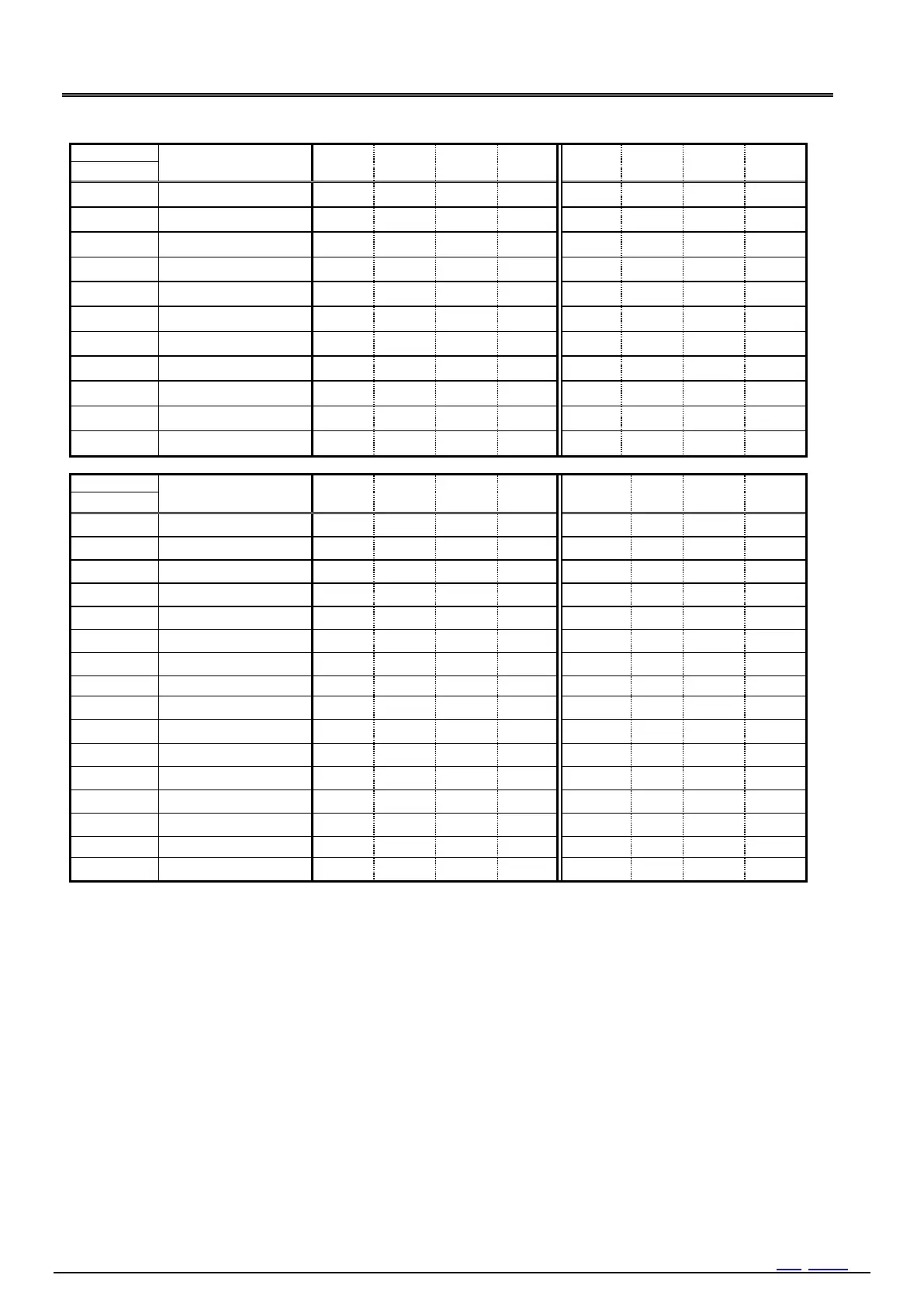
Table 13 Register Table 2
After the initial power-up (from 0 V) or in case the VLF bit returns 1, make sure to initialize all registers, before using the RTC.
Be sure to avoid entering incorrect date and time data, as clock operations are not guaranteed when the data or time data is
incorrect. Week data is not need care.
The TEST bit is used by the manufacturer for testing. Be sure to write 0 by initializing before using the RTC. Afterward, be sure to
set 0 when writing
Any bit marked with z should be used with a value of 0 after initialization. Writing 1 is ignored.
Any bit marked with is a RAM bit that can be used to read or write any data.
Write 0 - mark when writing. The read value is undefined. Please mask the corresponding bit after reading it.
The above table shows only the user registers. Due to functional reasons, RTC has different registers not mentioned above table
which are programmed by the manufacturer. Please make sure to only access above mentioned user registers.
Writing operation is i
0. Afterward, be kept in 0s possibility of current
consumption is increased.