9. Electrical Characteristics
RX4111CE Jump to Top / Bottom
ETM62E-02 Seiko Epson Corporation 12
9.2. AC characteristics
9.2.1. AC Characteristics (1)
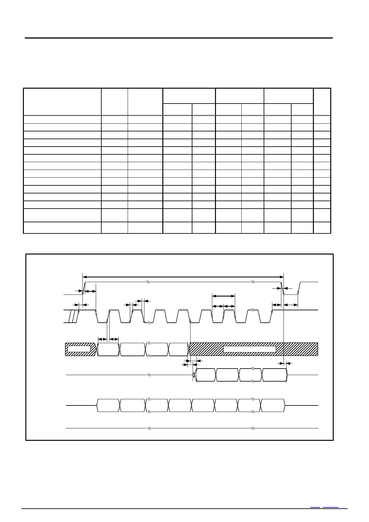
Table 7 AC Characteristics
Unless otherwise specified, GND = 0 V, V
IO
= 1.6 V 5.5 V, Ta = -40 C +85 C
DI/DO conflict avoiding time
10 for
Figure 13 SPI-Bus Timing Chart
Note: When writing data, it writes the data at CLK rise after received 8 bits of data in one time.
If communication is interrupted before receiving 8 bits data, data will not be written.
*1: Even if CE is Low, DI pin is active. Don't input half voltage and don't left open DI.