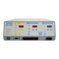
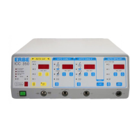
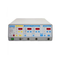
152 / 266 3CIRCUIT DESCRIPTION
QC power stage
Slot J4
The QC output stage (30128- 528)
The following functions are located on the PCB:
• Decoding of the switch signals
• Power-on time-delay circuit
• Preamplifier, driver and electrical isolation of actuation
• Clamping circuit
• Push-pull output stage.
The output stage acts as a power amplifier for high-frequency signals, as is required, for example, in switched-
mode power supply units and high-frequency surgical units. This output stage is designed for push-pull
operation on account of the greater efficiency and larger possible output power. As there are frequently
problems in procuring and storing identical P and N channel transistors - which are required for a push-pull
output stage - it is advantageous to be able to use two transistors of the same type. This circuit is then called
a quasi complementary output stage, or QC output stage for short.
The aim of the development was to produce an output stage with the highest possible efficiency and a
sinusoidal output signal with the smallest possible proportion of harmonic frequencies. Actuation should
require as low a power as possible and preferably be possible in digital mode so that the transistors can be
used in switching operation with low power loss.
All the stated requirements led to the present circuit.
Circuit principle
The complementary output stage consists of two N channel MOS-FET transistors, T1 and T2, which are
operated alternately as switches. The amplified digital output signal is present at the source of transistor T1
and simultaneously at the drain of transistor T2, since these connections are conductively connected to each
other. However, since a sinusoidal output signal is a required condition, the output of the output stage is
switched to an oscillating circuit (which is located on the next PCB).
The QC output stage is actuated between the gate and source of the respective transistor, which always
leads to electric potential problems with this circuit logic, since the actuation signal has to be superimposed
on the output signal.
This problem can be solved by actuating the relevant transistor via a transformer. If this method is used for
both output stage transistors, it has the advantage that the actuation circuit can be completely isolated from
the output circuit and the high output voltages occurring in the event of a defect cannot damage the actuation
circuit.
The disadvantage, however, is that the transformer cannot transmit any DC signals.
This is where the gate-source capacitance of the MOS-FETs proves useful. Since this capacitance is of high
quality, the gate-source capacitance can maintain an applied charge for a sufficient length of time. The
clamping circuit consisting of diodes D8, D9, D10 and D5, D6, D7 has the effect that the gate-source
capacitance can be charged with a short positive pulse. This positive pulse is fed via diode D8 to the gate of
transistor T1 and charges the GS capacitance sufficiently for the transistor to be switched to a conducting
state.