GE PROPRIETARY TO GE
D
IRECTION 5308917-100, REVISION 8 LOGIQ P3 SERVICE MANUAL
Chapter 5 Components and Functions (Theory) 5-17
5-2-5 Connector Board
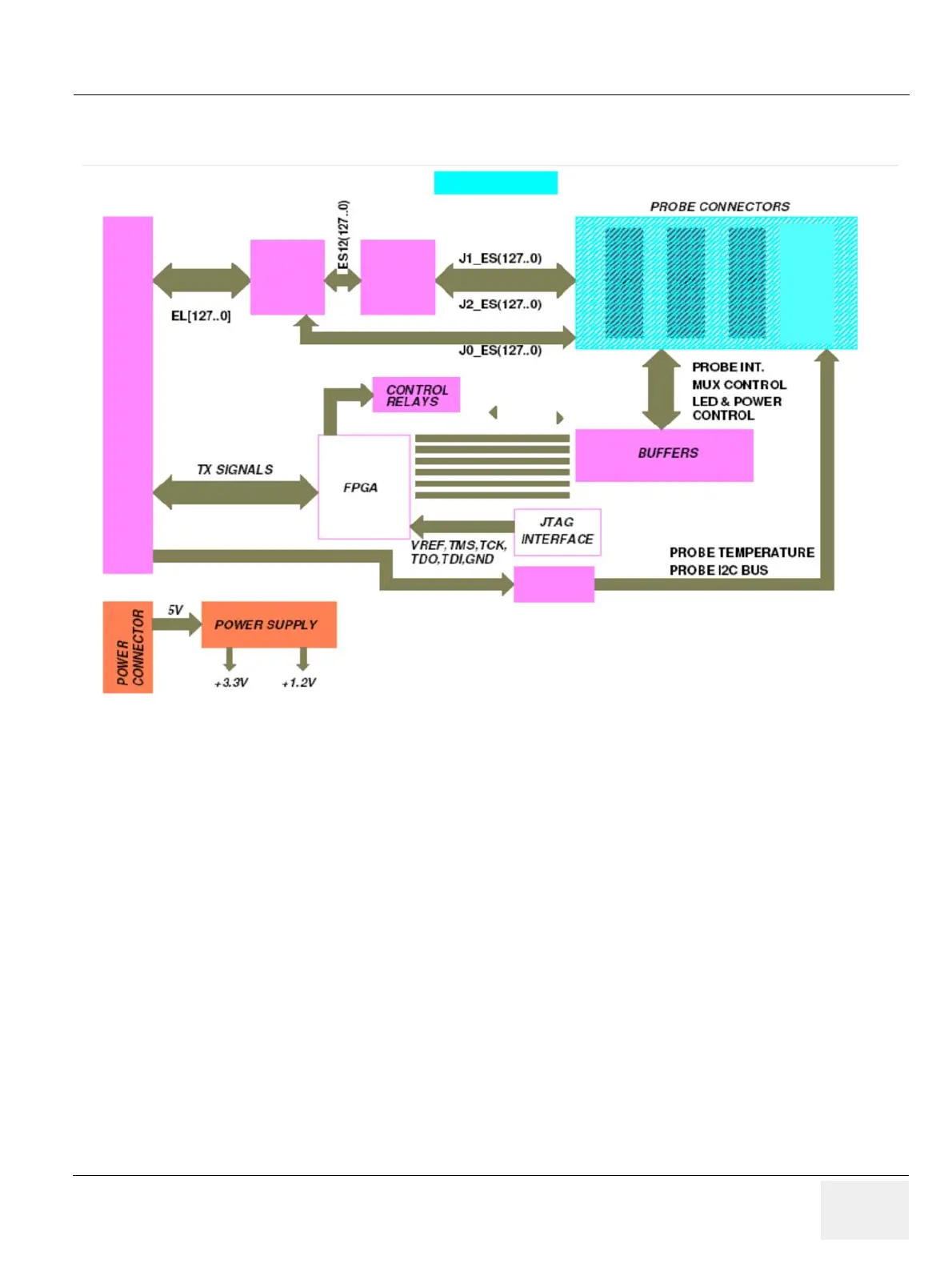
Figure 5-13 Connector Board Block Diagram
• There are 3 banks of relays on the Connector Board one each for each probe connector.
• There is one FPGA that acts like a buffer for the Probe related signals and is the interface between
the probe and the main TX Board FPGA. There is a I2C slave also implemented on this FPGA that
responds and interfaces with the Host I2C controller on the TX board it is mainly for probe selection
and control
• The Power supply to the TX board from the PDB board is connected via the Connector Board.
 Loading...