Function and Feature Description
Interface function Supports PHY-layer inloop.
Supports MAC-layer outloop.
Supports automatic loopback release at the port.
Clock Supports synchronous Ethernet.
Supports SSM protocol.
Supports IEEE 1588V2 protocol.
Supports 1588 ACR clock.
5.2.3 Working Principle and Signal Flow
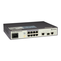
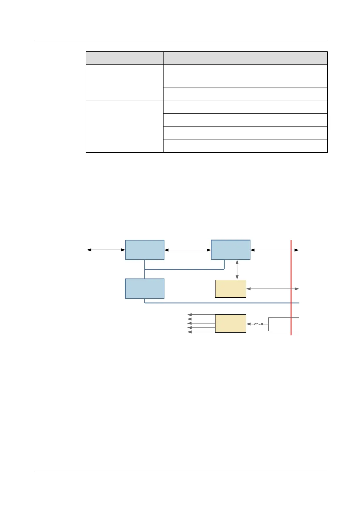
The AND1EM8T mainly consists of the service access module, service processing module,
management module, clock module, and power supply module.
Figure 5-3 shows the block diagram for the functions of the AND1EM8T.
Figure 5-3 Block diagram for the functions of the AND1EM8T
CXP
Service access
module
Clock
module
Service
processing
module
Management
module
8 x FE/GE
electrical signals
Service signals
Management bus
-48V/-60V
-48V/-60V
Power
supply
module
Back plane
Clock signals
CXP
CXP
Each module on the board
Service signals
Management bus
Management bus
Clock signals
System power
supply
System power
supply
3.0V
1.8V
2.5V
3.3V
1.2V
Transmit Direction
The service packets from AND1CXPA/AND1CXPB are sent to the service processing module
through the backplane-side interface of the AND1EM8T. The service processing module
identifies the destination interfaces for the packets, and buffers and schedules the packets. Then,
the service processing module sends the processed packets to the service access module, where
coding/decoding and serial/parallel conversion are performed. Finally, the service access module
outputs the packets through the GE/FE interfaces on the front panel.
Receive Direction
The GE/FE interfaces on the front panel receive GE/FE service signals. Then, the service access
module performs serial/parallel conversion and coding/decoding on the services, and then sends
ATN 950B Multi-service Access Equipment
Hardware Description 5 Physical Interface Card
Issue 03 (2012-07-23) Huawei Proprietary and Confidential
Copyright © Huawei Technologies Co., Ltd.
41
 Loading...