61IM483 Operating Instructions Revision R032306
P C B H o l e P a t t e r n
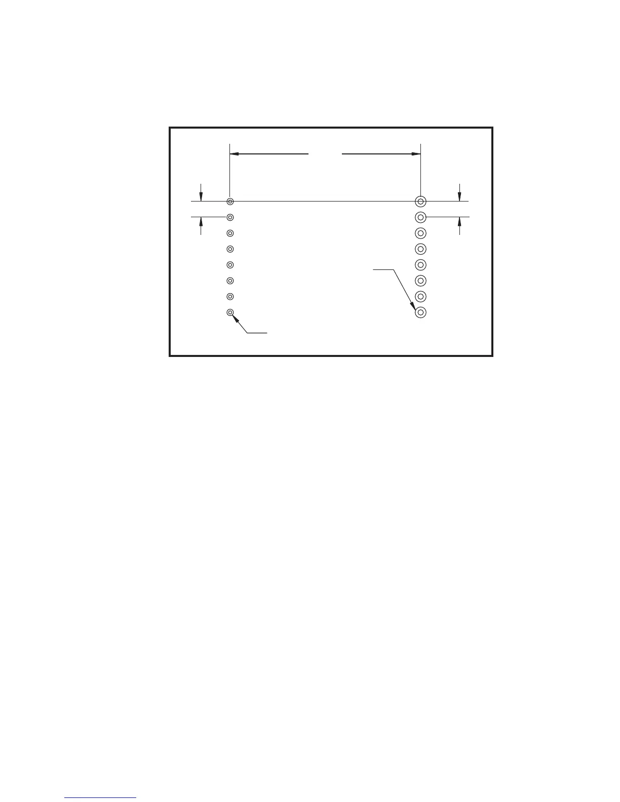
The IM483-8P2 is ideal for solder-mounting into a user’s PC board design.
Figure A.7 illustrates the PCB hole pattern as well as the recommended
hole and pad diameter for the IM483-8P2.
Figure A.7: IM483-8P2 PCB Hole Pattern
R e c o m m e n d e d S o l d e r i n g P r a c t i c e s
The following practices are recommended when solder mounting the
IM483-8P2 into your PCB:
R e c o m m e n d e d S o l d e r Te m p e r a t u r e
n 315°C (600°F)
R e c o m m e n d e d S o l d e r T i m e
n 10 Seconds
R e c o m m e n d e d S o l d e r s
n Kester “245” No-clean core solder.
n Alpha Metals “Telecore Plus Solder.
n Multicore “X39B” No-clean Solder.
n Or equivalent.
R e c o m m e n d e d S o l v e n t
n Tech Spray “Envirotech 1679”.
n Chemtronics “Flux-off NR 2000”.
n Or equivalent.