TLE5012B
Functional Description
User’s Manual 11 Rev. 1.2, 2018-02
2 Functional Description
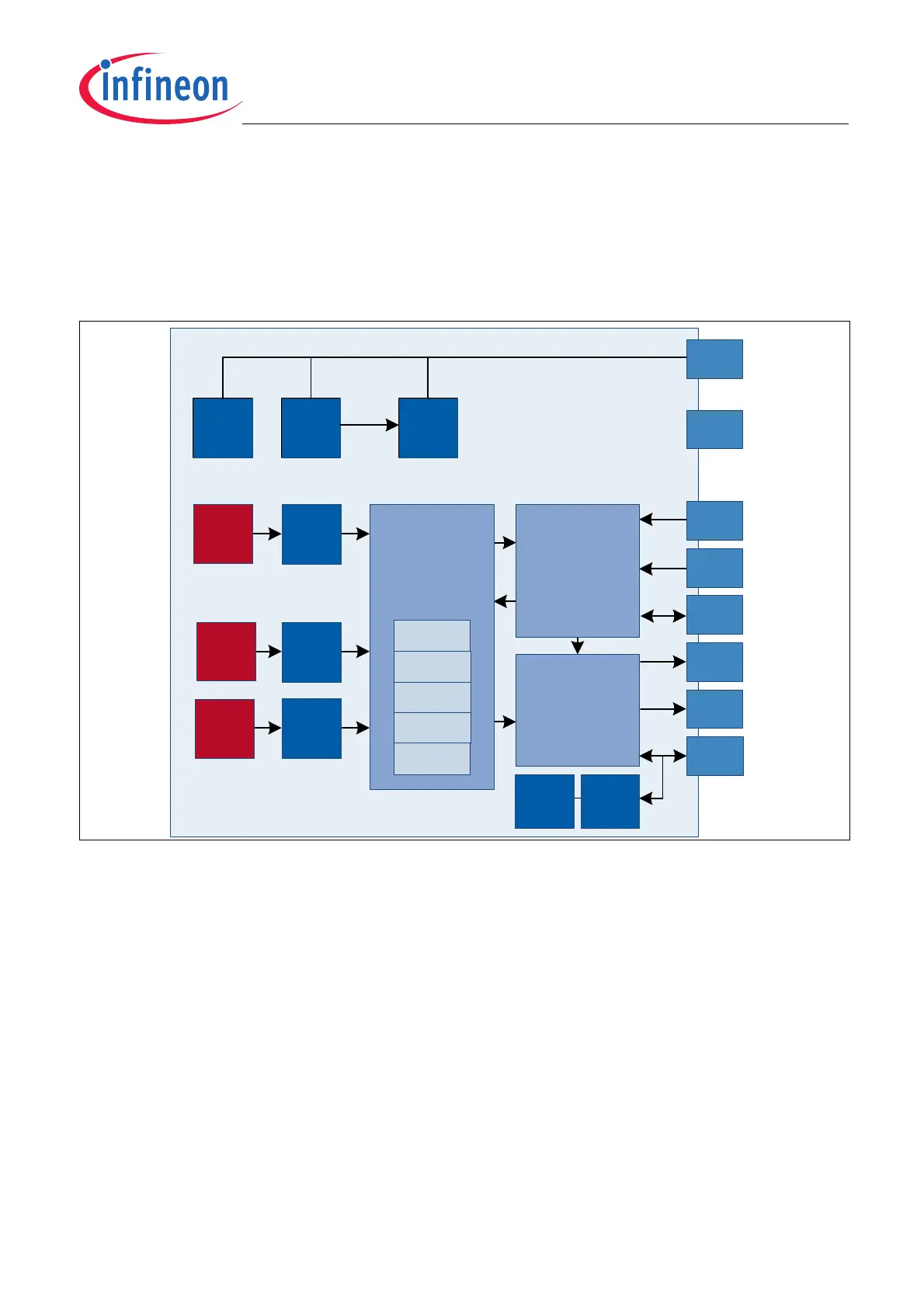
2.1 Block Diagram
Figure 2-1 TLE5012B block diagram
2.2 Functional Block Description
2.2.1 Internal Power Supply
The internal stages of the TLE5012B are supplied with several voltage regulators:
• GMR Voltage Regulator, VRG
• Analog Voltage Regulator, VRA
• Digital Voltage Regulator, VRD (derived from VRA)
These regulators are directly connected to the supply voltage V
DD
.
2.2.2 Oscillator and PLL
The digital clock of the TLE5012B is provided by the Phase-Locked Loop (PLL), which is by default fed by an
internal oscillator. In order to synchronize the TLE5012B with other ICs in a system, the TLE5012B can be
VRG VRA VRD
TLE5012B
V
DD
X
GMR
Y
GMR
Temp
SD-
ADC
SD-
ADC
SD-
ADC
Digital
Signal
Processing
Unit
CORDIC
CCU
RAM
SSC Interface
Incremental IF
PWM
HSM
SPC
CSQ
SCK
DATA
IFA
IFB
GND
IFC
Osc PLL
ISM
Fuses