TLE5012B
Interfaces
User’s Manual 35 Rev. 1.2, 2018-02
Data communication via SSC
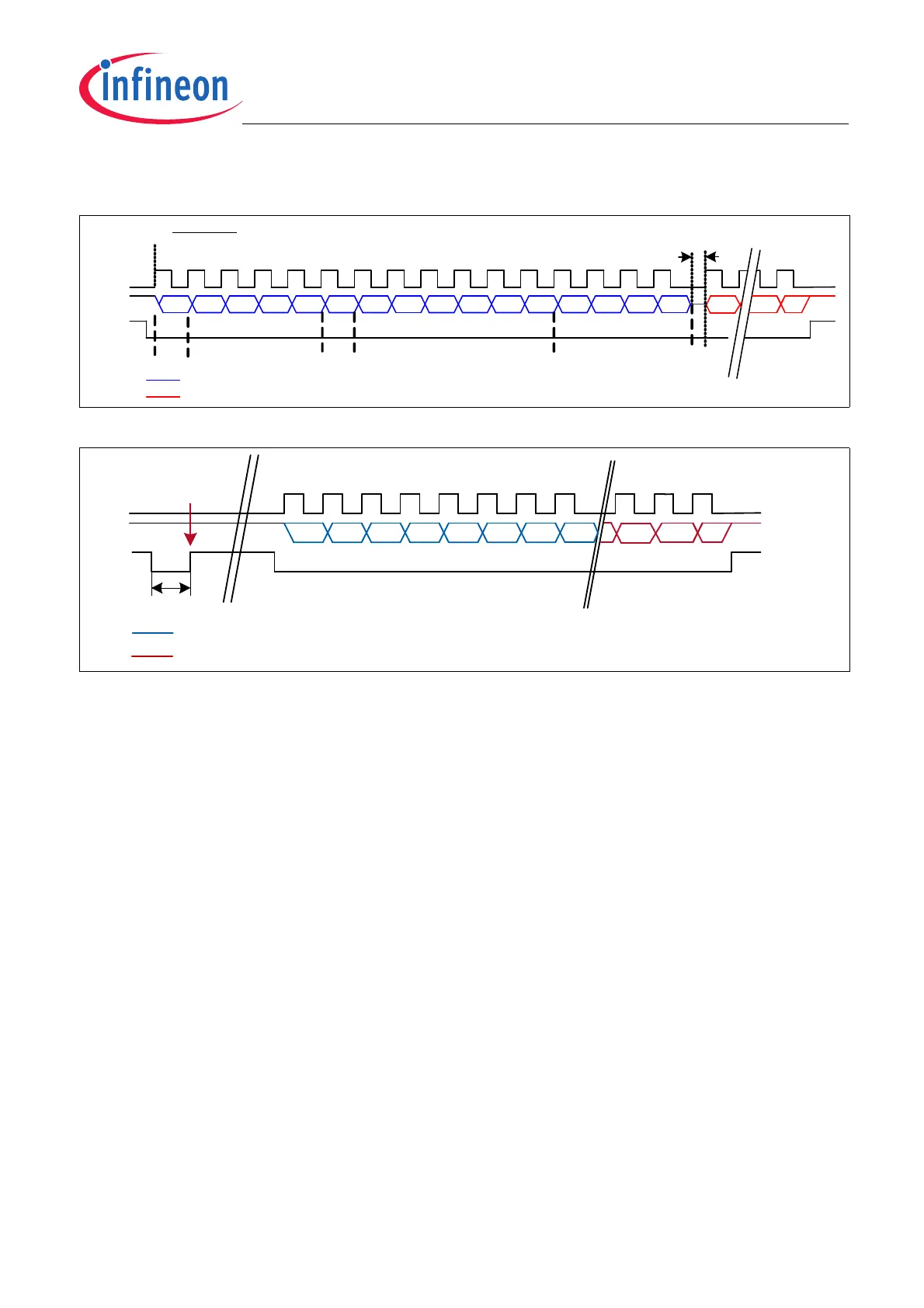
Figure 5-4 SSC bit ordering (read example)
Figure 5-5 Update of update registers
The data communication via SSC interface has the following characteristics:
• The data transmission order is Most-Significant Bit (MSB) first, Least-Significant Bit (LSB) last.
• Data is put on the data line with the rising edge of SCK and read with the falling edge of SCK.
• The SSC Interface is word-aligned. All functions are activated after each transmitted word.
• After every data transfer with ND 1, the 16-bit Safety Word is appended by the TLE5012B.
• A “high” condition on the Chip Select pin (CSQ) of the selected TLE5012B interrupts the transfer immediately.
The CRC calculator is automatically reset.
• After changing the data direction, a delay t
wr_delay
(see Table 5-3) has to be implemented before continuing the
data transfer. This is necessary for internal register access.
• If in the Command Word the number of data is greater than 1 (ND > 1), then a corresponding number of
consecutive registers is read, starting at the address given by ADDR.
• In case an overflow occurs at address 3F
H
, the transfer continues at address 00
H
.
• If in the Command Word the number of data is zero (ND = 0), the register at the address given by ADDR is
read, but no Safety Word is sent by the TLE5012B. This allows a fast readout of one register.
• At a rising edge of CSQ without a preceding data transfer (no SCK pulse, see Figure 5-5), the content of all
registers which have an update buffer is saved into the buffer. This procedure serves to take a snapshot of all
relevant sensor parameters at a given time. The content of the update buffer can then be read by sending a
read command for the desired register and setting the UPD bit of the Command Word to “1”.
• After sending the Safety Word, the transfer ends. To start another data transfer, the CSQ has to be deselected
once for at least t
CSoff
.
• By default, the SSC interface is set to push-pull. The push-pull driver is active only if the TLE5012B has to send
data, otherwise the DATA pin is set to high-impedance.
SCK
DATA 811 10 9MSB 14 13 12
CSQ
SSC Transfer
LSB3217 6 5 4
Command Wor d
Data Word (s)
SSC -Master i s dri ving D AT A
SSC -Slave is dr iving DAT A
LSB1
RW ADDR LENGTHLOC K
MSB
t
wr_delay
UPD
SCK
DATA
CSQ
LSB LSBMSB
Command W or d Data Word (s)Update -Signal
Update -Event
SSC -Master is driving DAT A
SSC -Slave is driving DAT A
t
CSupdate