TLE5012B
Application Circuits
User’s Manual 17 Rev. 1.2, 2018-02
3 Application Circuits
The application circuits in this chapter show the various communication possibilities of the TLE5012B. The pin
output mode configuration is device-specific and it can be either push-pull or open-drain. The bit IFAB_OD
(register IFAB, 0DH) indicates the output mode for the IFA, IFB and IFC pins. The SSC pins are by default push-
pull (bit SSC_OD, register MOD_3, 09H). Every application circuits below are using otherwise specified SSC with
push-pull configuration and the internal clock.
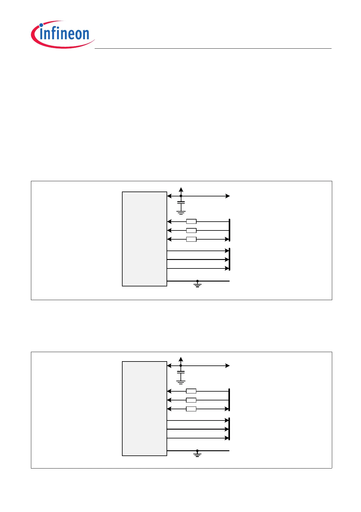
3.1 IIF interface and SSC (IIF in push-pull configuration)
Figure 3-1 shows a block diagram of a TLE5012B with Incremental Interface (IIF) and SSC interface. The derivate
TLE5012B - E1000 is by default configured with push-pull IFA (IIF_A), IFB (IIF_ B) and IFC (IIF_IDX) pins. When
the output pins are configurated as open-drain, three pull-up resistors should be added (e.g. 2k2Ω) between the
data lines and VDD.
Figure 3-1 Application circuit for TLE5012B with IIF interface and SSC
3.2 HSM interface and SSC (HSM in push-pull configuration)
Figure 3-2 shows a block diagram of the TLE5012B with Hall Switch Mode (HSM) and SSC interface. The derivate
TLE5012B - E3005 is by default configurated with push-pull IFA (HS1), IFB (HS2) and IFC (HS3) pins.
Figure 3-2 Application circuit for TLE5012B with HSM interface (push-pull configuration) and SSC
TLE5012B
CSQ
SCK
DATA
IFA
IFB
IFC
GND
VDD
3.0 – 5.5V
Rs1
SSC
IIF
100nF
(IIF_A)
(IIF_B)
(IIF_IDX)
Rs1
Rs2
Rs1 recommended, e.g. 100
Rs2 recommended, e.g. 470
TLE5012B
CSQ
SCK
DATA
IFA
IFB
IFC
GND
VDD
3.0 – 5.5V
Rs1
SSC
HSM
100nF
(HS1)
(HS2)
(HS3)
Rs1
Rs2
Rs1 recommended, e.g. 100
Rs2 recommended, e.g. 470