TLE5012B
Functional Description
User’s Manual 16 Rev. 1.2, 2018-02
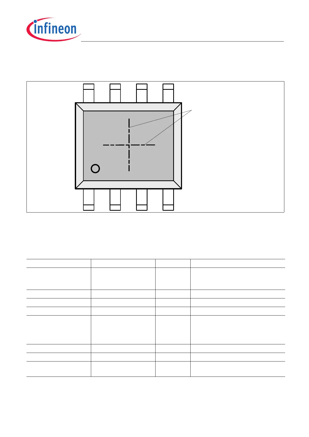
2.4 Pin Configuration
Figure 2-6 Pin configuration (top view)
2.5 Pin Description
Table 2-1 Pin Description
Pin No. Symbol In/Out Function
1IFC
(CLK / IIF_IDX / HS3)
I/O Interface C:
External Clock
1)
/ IIF Index / Hall Switch
Signal 3
1) External clock feature is not available in IIF or HSM interface mode
2 SCK I SSC Clock
3 CSQ I SSC Chip Select
4 DATA I/O SSC Data
5IFA
(IIF_A / HS1 / PWM / SPC)
I/O Interface A:
IIF Phase A / Hall Switch Signal 1 /
PWM / SPC output (input for SPC trigger
only)
6V
DD
- Supply Voltage
7GND-Ground
8IFB
(IIF_B / HS2)
O Interface B:
IIF Phase B / Hall Switch Signal 2
12 34
5678
Center of Sensitive
Area