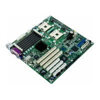
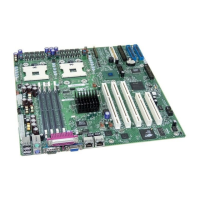
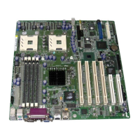
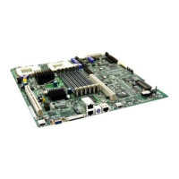
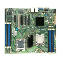
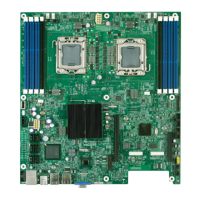
Intel® Server Board SE7520BD2 Technical Product Specification Environmental Specifications
Revision 1.3 Intel Confidential 149
7.2.3 Standby Powered Device Map
The following components on the Server Board SE7520BD2 require standby power when the
system is in S4 or S5 sleep states:
• Server I/O: +3.3VSB
• Heceta 7: +3.3VSB
• All PCI/PCI-X slots: +3.3VSB
• All PCI Express slots: +3.3VSB
• Serial Port RS232 Converter : +5VSB
• ICH5-R: +3.3VSB, SB1_5V (internally generated on ICH5-R), +5VSB
• SM connector: +3.3VSB, +5VSB
• Battery circuit: +3.0VSB
7.2.4 System Reset Block Diagram
Note: Getting CPU_VRD_PWR_GD input to the ICH5-R VRMPWRGD adds redundant logic as
the CPU_VRD_PWR_GD is also routed to the ICH5-R PWROK. The RTC power well isolation
circuit for the RSMRST_N is NOT shown in the following diagram for simplicity. The Heceta 7
RESET _N is output on power up with an ~200ms delay and input after power on. The power
ON reset also sets all Heceta 7 registers to their default values. Added the RSMRST_N
generation circuitry (empty sites) shown in ICH5 DG. This circuitry will be required if the Heceta
7 is NOT available for power-ON.
There is a 1msec delay from the VTT_PWRGD generated from the P_VTT (1.2V) regulator
power good signal to the SB_VTT_PWRGD, which is used for generating the VID_PWRGD for
the CPUs. Similarly, there is a 1msec delay from the time the SB_VTT_PWRGD is generated to
VR0_SYS_ENABLE. These details are not shown in the following diagram. This delay logic is
inside the PLD.
The Intel® Xeon™ processor/E7520 platform power sequence is as follows:
1. Chipset (MCH, PXH, ICH5-R) and processors are powered up.
2. On-die power-detect circuitry initiates PLL locking. However, the absence of the
reference clock at PLL input triggers the Low Frequency detect circuit, which shuts
the PLL off.
3. Reference clocks are driven from the clock chips (CK409B/DB800). The clock chips
drive output clocks only after the PLLs in these chips have locked. That is, they only
drive good clocks.
4. Presence of a reference clock is detected by the Low Frequency Detect Circuit. PLL
locking is re-initiated.
5. PLLs locked.
6. Chipset (MCH, PXH, ICH5-R) and processors receive external PowerGood.
7. FSB VTT regulator power good to CPU VIDPWRGD delay needs to be 1msec to
10msec.
8. CPUVIDPWRGD to CPU Vcore delay needs to be at least 1msec.