Environmental Specifications Intel® Server Board SE7520BD2 Technical Product Specification
150 Intel Confidential Revision 1.3
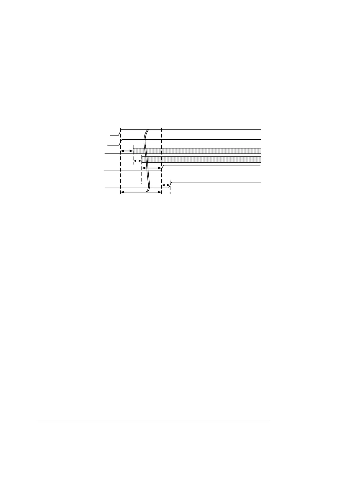
Additional Details: SB_VTT_PWRGD is a delayed copy (minimum 1msec) of FSB VTT
regulator VTT_PWRGD when the VTT_PWRGD transitions from low to high.
VR0_SYS_ENABLE is generated based on the glue logic shown in the PLD plus
SB_VTT_PWRGD plus an additional minimum 1msec delay. This delay logic is inside the PLD.
Figure 17. Reset and PowerGood Timings
7.2.4.1 Power Sequencing Diagram
The Power Good signal from the power supply starts the reset sequence in the system. The
intent of the power good signal and the reset sequence is to ensure that all components are
held in reset mode until power (and system clocks) have stabilized. The power good signal from
the power supply will go true after all the output voltages have reached specified levels. Power
Good will go false just previous to any voltage dropping below the specified level. Refer to the
EPS12V Power Supply Specification for further details.
All VRs PowerGood
CPU_VRD_PWR_GD
SYS_PWR_GD_3_3V
PCIRST_N
CK409B Stable Output Clocks
DB800 Stable Output Clocks
VALID Clocks
VALID Clocks
1.8ms
(max)
1ms
(max)
100ms
1ms