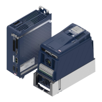
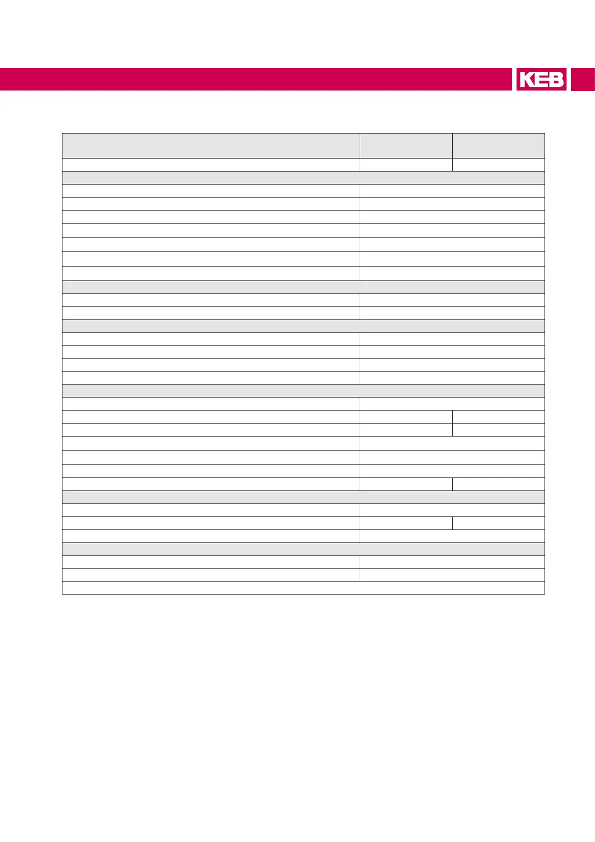
3.2.1 Technical data of the charging units H6
Device size
00
Version 1
00
Version 2
Housing B / P B / P
Input data
Rated input voltage U
N / V 400(UL:480)
Input voltage range U
in / V 320…480
Mains frequency f
N / Hz 50/60±2
Mains phases 3
Approved mains forms TN
Max. permissible mains fuse I
_max / A 10
Supply cable section Ø / mm² 1.5
DC output data
Output voltage range U
_dc / V 452…840
Rated output current I
outN_dc / A 20
Output data precharging
Rated output voltage U
outN_dc / V 565
Output voltage range U
_dc / V 452…680
Overvoltageswitch-o U
OP_dc / V 840
Max. precharging current I
O_dc / A 5
Braking transistor (GTR7)
Max.brakepower(switchingcycle=40%) P
_max / kW 46.2
Max. braking current IB
_max_dc / A 146 176
Min. braking resistor
RB_min
/Ω 6(-10%) 5(-10%)
Connection cross section mm² 16
Response voltage U
_dc / V 780
Switching frequency f
SN / kHz 4
Switchingcyclebasedon120scycletime ED /% 40 30
Other data
Power dissipation interior P
Dint / W 5
Max. heat sink temperature THS /°C 80 60
Insulation resistance @ U
dc=500V Rsio/MΩ > 5
Supply control unit
Input voltage U
CU_dc / V 24(±10%)
Input current
1)
ICU_dc / A 0.2
Table 8: Technical data of the charging modules H6
1)
Input current, if no digital input is set. At max. load at the digital outputs the input current can be increased
up to max. 1 A.
29
TECHNICAL DATA OF THE AIC MODULES
 Loading...