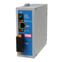
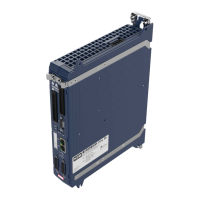
View upper side of the device
X4B
X4C
X4A
X2D
X2C
X2A
Digital inputs and outputs
X2A
Dig. input 4 16 15 24V/<0.7Adcoutput
Dig. input 3 14 13 24V/<0.7Adcoutput
Dig. input 2 12 11 24V/<0.7Adcoutput
Dig. input 1 10 9 24V/<0.7Adcoutput
Dig. output 4 8 7 0V
Dig. output 3 6 5 0V
Dig. output 2 4 3 0V
Dig. output 1 2 1 0V
X2C
Error chain 2 1
Charging status of the DC link
and error output of the axis
modules
X2D
Error chain 2 1
X4A
reserved 1
6 reserved
TxD (RS232) 2
7 DGND (reference potential)
RxD (RS232) 3
8 TxD-A(RS485)
RxD-A(RS485) 4
9 TxD-B(RS485)
RxD-B(RS485) 5
X4C
no function
X4B
no function
Figure 26: View upper side of the device
53
INSTALLATION AND CONNECTION
 Loading...