8.5 Single-board version with housing (mvBlueFOX-IGC2xx) 69
8.5.3 Positioning tolerances of sensor chip
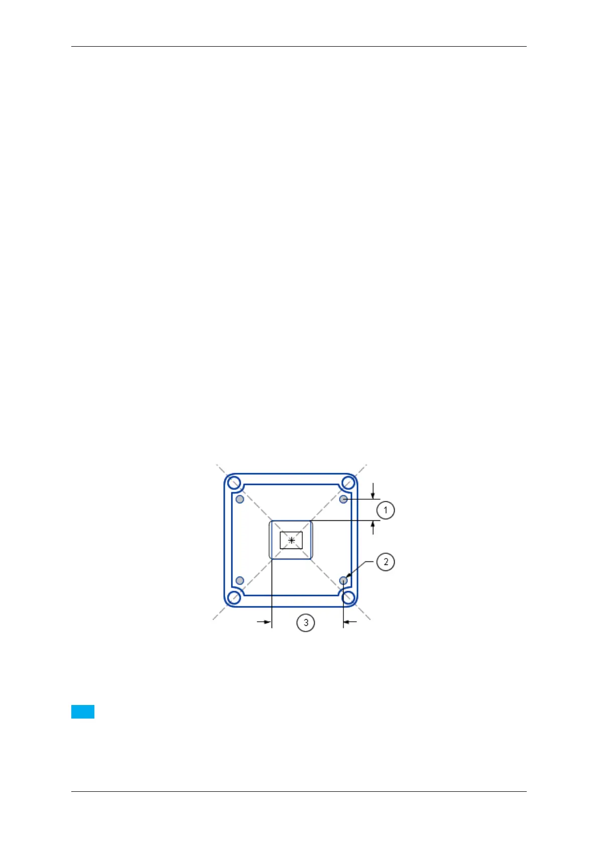
The sensor's optical midpoint is in the center of the housing. However, several positioning tolerances in relation to
the housing are possible because of:
• Tolerance of mounting holes of the printed circuit board in relation to the edge of the lens holder housing is
not specified but produced according to general tolerance DIN ISO 2768 T1 fine.
• Tolerance of mounting holes on the printed circuit board because of the excess of the holes ± 0.1 mm (Figure
32; 2).
• Tolerance between conductive pattern and mounting holes on the printed circuit board.
Because there is no defined tolerance between conductive pattern and mounting holes, the general defined
tolerance of ± 0.1 mm is valid (Figure 32; 1 in the Y-direction ± 0.1 mm; 3 in the Z-direction ± 0.1 mm)
There are further sensor specific tolerances, e.g. for model mvBlueFOX-IGC200wG:
• Tolerance between sensor chip MT9V034 (die) and its package (connection pad)
– Chip position in relation to the mechanical center of the package: 0.2 mm (± 0.1mm) in the X- and
Y-direction (dimensions in the sensor data sheet according to ISO 1101)
• Tolerance between copper width of the sensor package and the pad width of the printed circuit board
During the soldering the sensor can swim to the edge of the pad: width of the pad 0.4 mm (possible tolerance
is not considered), width of pin at least 0.35 mm, max. offset: ± 0,025mm
Further specific tolerances of other models on request.
Figure 32: Positioning tolerances of sensor chip
Note
There are also tolerances in lens which could lead to optical offsets.
MATRIX VISION GmbH