188
Note
The output voltage offset function is enabled only under the V/F mode.
D: Output voltage
When this function is enabled under V/F mode, the drive output voltage VO and the output frequency are
mutually independent. The drive output voltage is not restricted by the V/F feature curve of Group P07,
but is determined by the analog input signal, as shown in Fig.6-50.
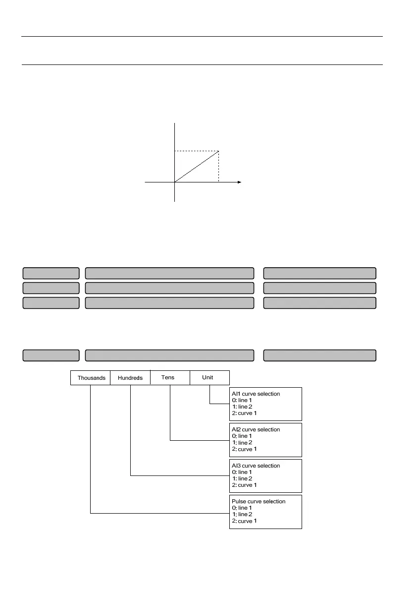
AI
min
Analog voltage
AI
max
Output voltage Vo
V
max
0V
Fig. 6-50 Output voltage curve
The horizontal coordinate in the figure is the adjusted analog input signal, the vertical coordinate is the
drive output voltage value. When the input analog voltage is less than 0, the output voltage is 0.
E: Reserved
P10.02~P10.04 defines the channel filtering time constant for the filtering of the input signal. The longer
the filtering time is, the stronger the immunity becomes, but the slower the response will become. The
shorter the filtering time is, the faster the response becomes, but the weaker the immunity will become.
Fig. 6-51 Analog and pulse curve selection
Analo
curve selection 0~2222H
0210H
P10.05
AI3 filterin
time 0.000~10.000s
0.010s
P10.04
AI2 filterin
time 0.000~10.000s
0.010s
P10.03
AI1 filterin
time 0.000~10.000s
0.010s
P10.02
 Loading...