7
4. Connecting method
4−1. Layout of terminals and BCD output connector
There are 2 pieces of terminals, one has 11 pieces of terminal points (Terminals 1)
and the other has 3 pieces of terminal points (Terminals 2) and also attached BCD output
connector.
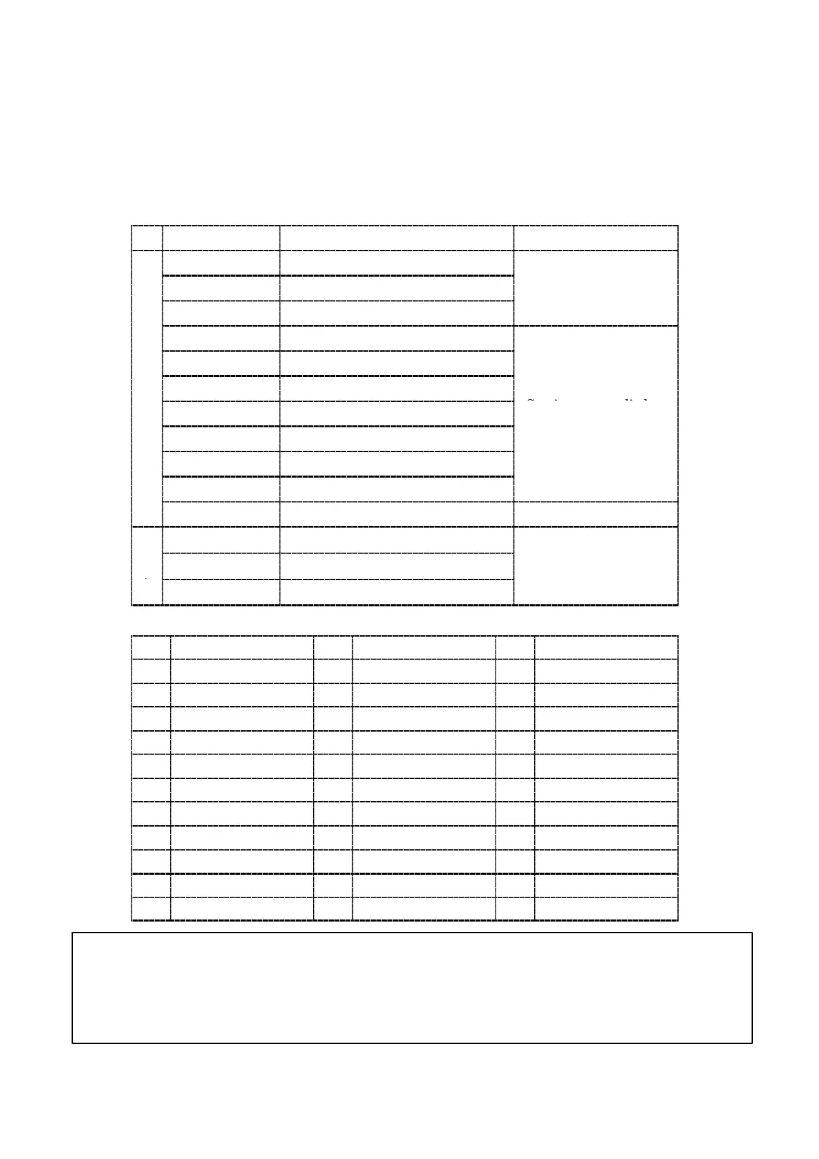
Layout of terminals and BCD output connector are shown in the following figure.
D Terminals
Terminal NO. Name Applications
1 DC24 V(+)
2 DC24 V(−)
Power supply
3 GND
4 A (Bridge power supply +)
ls 1
5 F (Sensing +)
ina
6 G (Sensing −)
er
7 C (Bridge power supply −)
Strain gage applied
8 D (Amplifier input +)
9 B (Amplifier input −)
10 E (Shield)
11 A.G.
Analog ground
l2
1 RUN
mina
2 ERROR
Open collector output
Ter
3 COM.
D BCD output connector
1
COM. 13 8×10
2
25 ERROR
2 1×10
0
14 1×10
3
26 P.C.
3 2×10
0
15 2×10
3
27 HOLD
4 4×10
0
16 4×10
3
28 LOCK
5 8×10
0
17 8×10
3
29 SEL.1
6 1×10
1
18 1×10
4
30 SEL.2
7 2×10
1
19 COM. 31 ZERO
8 4×10
1
20 2×10
4
32 A/Z
9 8×10
1
21 4×10
4
33 A/Z OFF
10 1×10
2
22 8×10
4
34 N.C.
11 2×10
2
23 POL. 35 N.C.
12 4×10
2
24 OVR. 36 N.C.
● Don’t connect with the N.C. pin at the BCD output connector.
● The COM. on the terminals 2 and COM. on BCD output connector
are connected internally.


 To Next Page