53
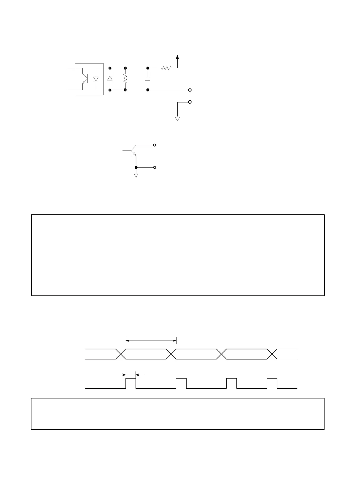
7−2−4. Equivalent circuit for input/output
(1) Equivalent circuit for input section
+5V
470Ω
INPUT
COM.
680Ω
0.1μ
(2) Equivalent circuit for output section
COM.
OUTPUT
V
CE
=DC30 V,Ic=20 mA MAX.
7−2−5. Timing chart
Warning ● When reading each output data of BCD output through sequencer
and so on, read with the timing that P.C.(Print command) is “at the
edge from ON to OFF”. Moreover, take full consideration on “Input
response delay time” for reading instrument such as sequencer and so
on. If neglected, there may have the case that reading data is not
performed correctly.
(1) Normal
DATA
POL.
ON
P.C.
50 times/s:Approx.20 ms
20 times/s:Approx.50 ms
4 times/s:Approx.250 ms
Changeable into approx. 5 ms, approx. 15 ms and
approx. 100 ms. with the dip switch.
ON
ON
ON
ON
ONON
ON
● At the time of data output of all of P.C., DATA and POL., output
transistor will be ON (Negative logic electrically.).