54
(2) When data is over.
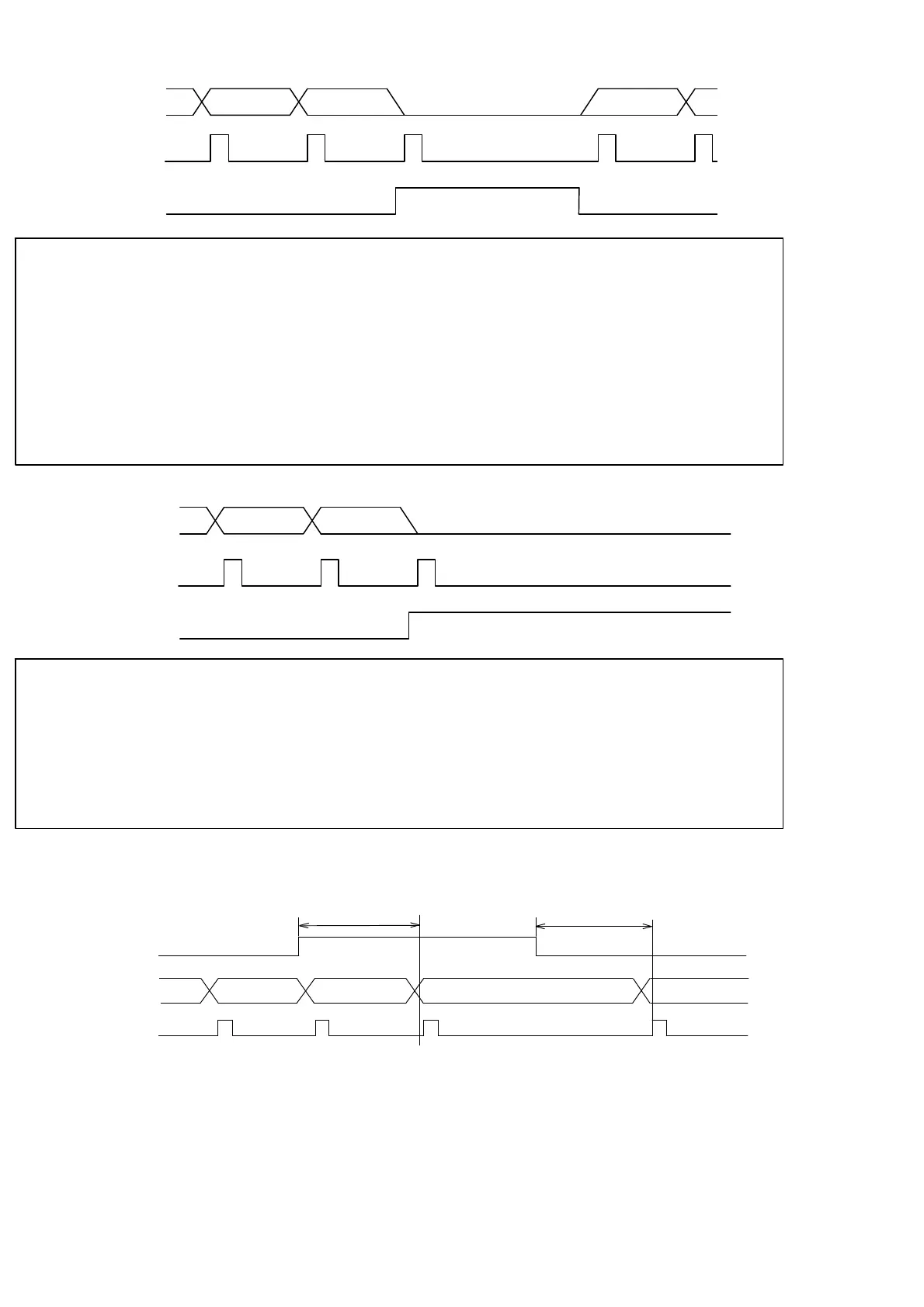
DATA
POL.
P.C.
ON
OVR.
ON
ON
ON
ON
ON
● At the time of OVR output, output transistor of OVR signal will
become ON (Negative logic electrically). Moreover, all of P.C., DATA
and POL. will OFF condition of output transistor at the time of
ERROR output(Positive logic electrically).
(As for P.C., it will be OFF after one shot of operation, and POL. will
be normal OFF at the time of “OL”, and normal ON at the time of
“−OL”.)
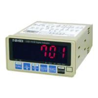
(3) In case of occurrence of error
DATA
POL.
P.C.
ON
ERROR
ON
ON
ON
● Output transistor of ERROR signal will become ON (Negative logic
electrically) at the time of ERROR output. Moreover all of P.C., DATA
and POL. will be OFF condition of output transistor at the time of
ERROR output. (Positive logic electrically)
(As for P.C., it will be OFF after one shot of operation is over.)
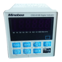
(4) At the time of HOLD signal input
DATA
POL
P.C.
HOLD
ON
ON
4 times/s : Approx. 350 ms at Max.
20 times/s : Approx. 150 ms at Max.
50 times/s : Approx. 120 ms at Max.
4 times/s : Approx. 350 ms at Max.
20 times/s : Approx. 150 ms at Max.
50 times/s : Approx. 120 ms at Max.