EasyManuals Logo

Quectel 5G Series Hardware Design

Quectel 5G Series
86 pages
To Next Page IconTo Next Page
To Previous Page IconTo Previous Page
Page #29 background imageLoading...
Page #29 background image
5G Module Series
RM500Q-GL Hardware Design
RM500Q-GL_Hardware_Design 28 / 85
Module
ET
2, 4
C2
220 μF
3, 5, 11
VCC (3.7 V Typ.)
VCC
GND
C10
10 pF
C8
33 pF
C6
100 nF
C4
1 μF
+
C1
220 μF
D1
5.1 V
VCC
GND
C9
10 pF
C7
33 pF
C5
100 nF
C3
1 μF
+
27, 33, 39,
45, 51, 57,
71, 73
70, 72, 74
PMU
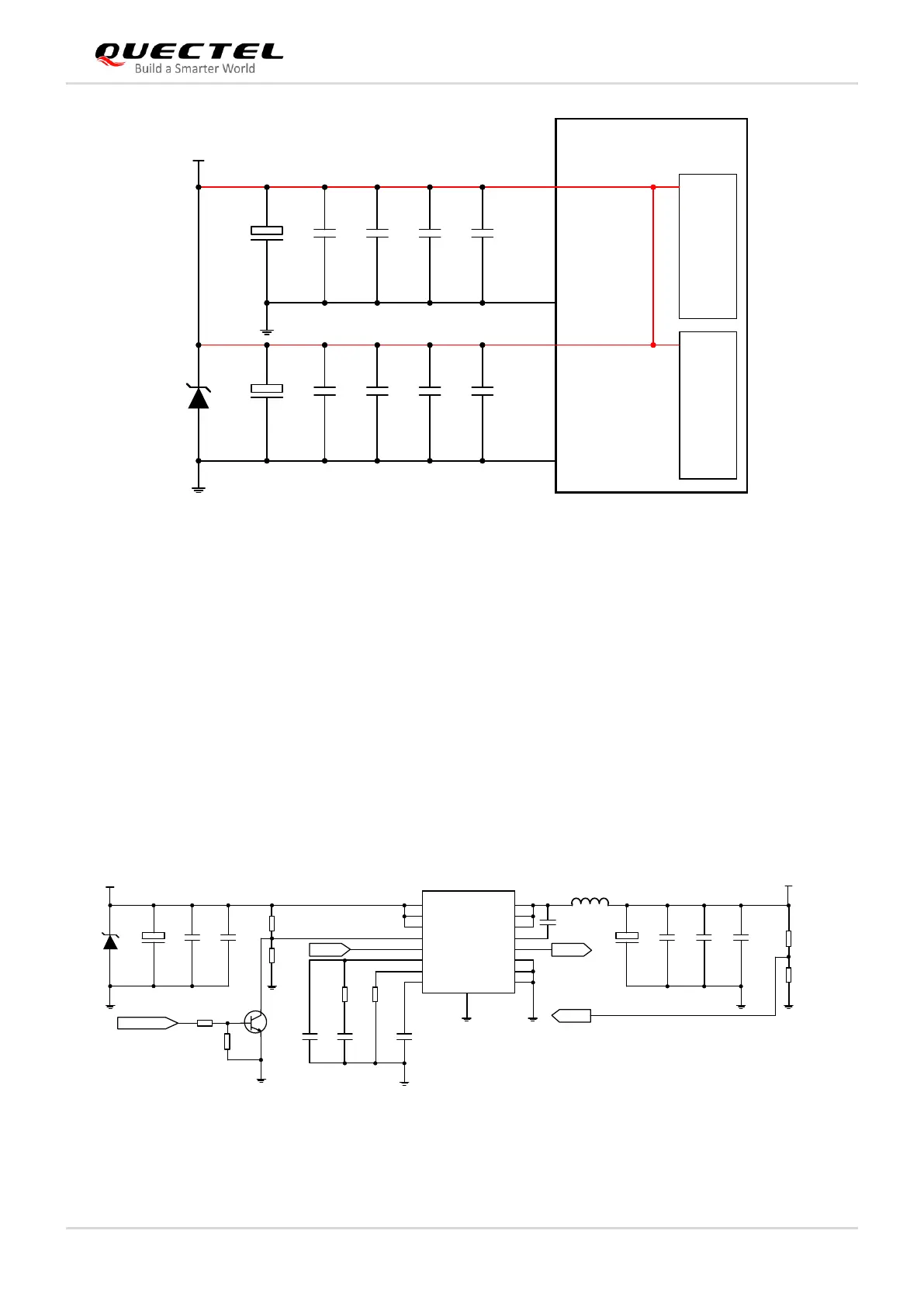
Figure 6: Reference Circuit for VCC Pins
3.3.2. Reference Design for Power Supply
Power design is critical as the modules performance largely depends on its power source. The power
supply of the module should be able to provide a sufficient current of 3.0 A at least. If the voltage
difference between input and output is not too big, use an LDO when supplying power to the module. If
there is a big voltage difference between the input source and the desired output (VCC = 3.7 V typical), a
buck DC-DC converter is preferred.
The following figure shows a reference design for +5.0 V input power source based on the DC-DC
converter. The typical output of the power supply is about 3.7 V and the maximum load current is 3.0 A.
D1
TVS
PWR_IN
C8
220 μF
C11
10 pF
C10
33 pF
C9
100 nF
+
R1
205k
U1
Q1
NPN
R8
47k
R7
4.7k
PWR_EN
R4
182k
PWR_OUT
L1
1.5 μH
VIN
VIN
VIN
EN
VSNS
COMP
RT/CLK
SS
PH
PH
PH
BOOT
PWRGD
GND
GND
AGND
VFB
R5
383k 1%
R6
100k 1%
C6
100 nF
PWRGD
EP
R2
80.6k
C7
10 nF
R3
10k
C4
10 nF
C5
NM
VFB
C2
100 nF
C3
33 pF
C1
470 μF
+
Figure 7: Reference Design for Power Supply

Table of Contents

Other manuals for Quectel 5G Series

Questions and Answers:

Question and Answer IconNeed help?

Do you have a question about the Quectel 5G Series and is the answer not in the manual?

Quectel 5G Series Specifications

General IconGeneral
BrandQuectel
Model5G Series
CategoryControl Unit
LanguageEnglish

Related product manuals