5G Module Series
RM500Q-GL Hardware Design
RM500Q-GL_Hardware_Design 44 / 85
4.3.3. Reference design for PCIe
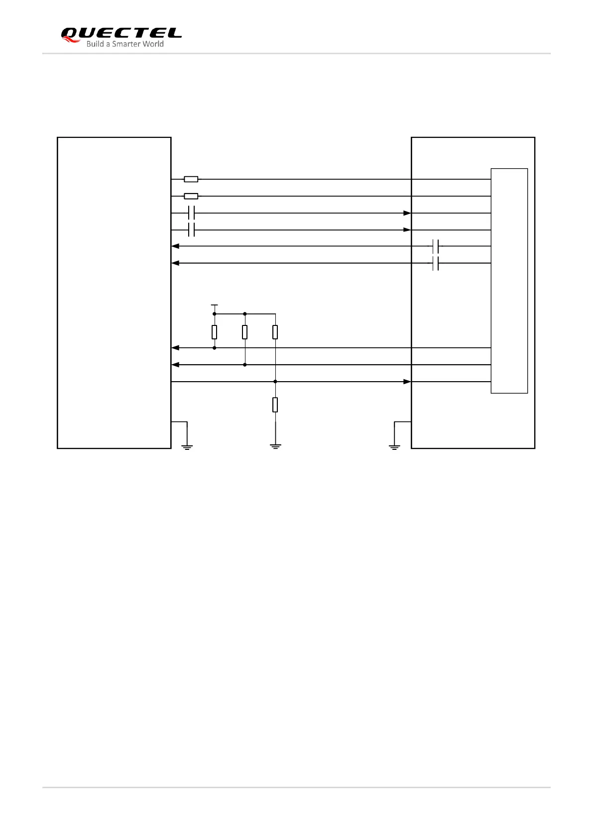
The following figure shows a reference circuit for the PCIe interface.
Figure 19: PCIe Interface Reference Circuit
To ensure the signal integrity of PCIe interface, AC coupling capacitors C3 and C4 should be placed close
to the host on PCB. C1 and C2 have been integrated inside the module, so do not place these two
capacitors on your schematic and PCB.
The following principles of PCIe interface design should be complied with to meet the PCIe specification.
⚫ Keep the PCIe data and control signals away from sensitive circuits and signals, such as RF, audio,
crystal and oscillator signals.
⚫ Add a capacitor in series on Tx/Rx traces to prevent any DC bias.
⚫ Keep the maximum trace length less than 300 mm.
⚫ Keep the length matching of each differential data pair (Tx/Rx) less than 0.7 mm for PCIe routing
traces.
⚫ Keep the differential impedance of PCIe data trace as 85 Ω ±10 %.
⚫ You must not route PCIe data traces under components or cross them with other traces.
 Loading...