EasyManuals Logo

Quectel 5G Series Hardware Design

Quectel 5G Series
86 pages
To Next Page IconTo Next Page
To Previous Page IconTo Previous Page
Page #51 background imageLoading...
Page #51 background image
5G Module Series
RM500Q-GL Hardware Design
RM500Q-GL_Hardware_Design 50 / 85
4.5.2. W_DISABLE2#
RM500Q-GL provides a W_DISABLE2# pin to disable or enable the GNSS function. The W_DISABLE2#
pin is pulled up by default. Driving it low will disable the GNSS function. The combination of
W_DISABLE2# pin and AT commands controls the GNSS function.
Table 22: GNSS Function Status
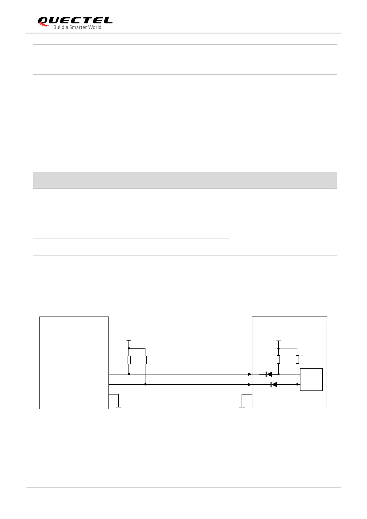
A simple level shifter based on diodes is used on W_DISABLE1# pin and W_DISABLE2# pin which are
pulled up to a 1.8 V voltage in the module, as shown in the following figure, so the control signals (GPIO)
of the host device could be 1.8 V or 3.3 V voltage level. W_DISABLE1# and W_DISABLE2# are active
LOW signals, and a reference circuit is presented below.
Host Module
W_DISABLE2#
W_DISABLE1#
BB
GPIO
GPIO
26
8
VDD 1.8 V
R3
10k
R4
10k
NOTE: The voltage level of VCC_IO_HOST could be 1.8 V or 3.3 V typically.
VCC_IO_HOST
R1
100k
R2
100k
Figure 24: W_DISABLE1# and W_DISABLE2# Reference Circuit
Low
AT+CFUN=0
AT+CFUN=1
AT+CFUN=4
Disabled
W_DISABLE2# Logic Level
AT Commands
GNSS Function Status
High
AT+QGPS=1
Enabled
High
AT+QGPSEND
Disabled
Low
AT+QGPS=1
Low
AT+QGPSEND

Table of Contents

Other manuals for Quectel 5G Series

Questions and Answers:

Question and Answer IconNeed help?

Do you have a question about the Quectel 5G Series and is the answer not in the manual?

Quectel 5G Series Specifications

General IconGeneral
BrandQuectel
Model5G Series
CategoryControl Unit
LanguageEnglish

Related product manuals