5G Module Series
RM500Q-GL Hardware Design
RM500Q-GL_Hardware_Design 31 / 85
Table 9: Turn-on Timing of the Module
3.5. Turn off
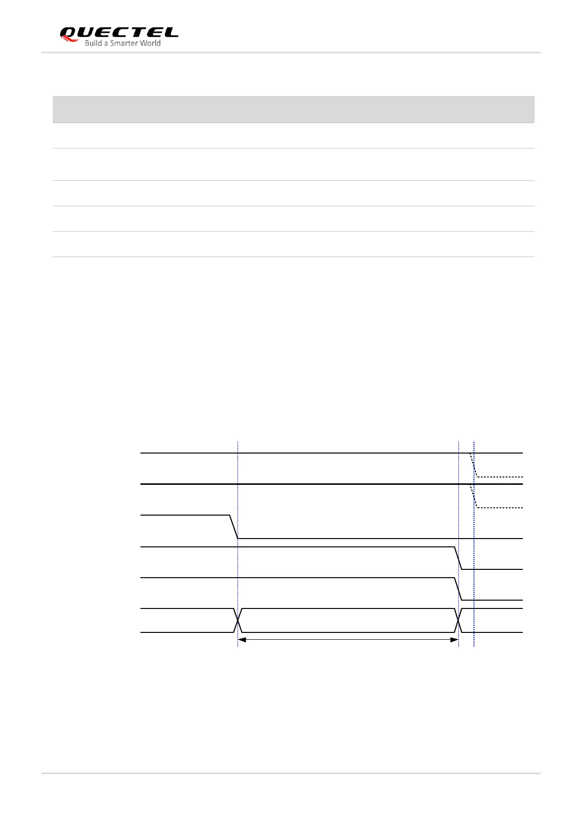
3.5.1. Turn off the Module Through FCPO#
For the design that turns on the module with a host GPIO, when the power is supplied to VCC, driving
FULL_CARD_POWER_OFF# pin LOW (≤ 0.2 V) or tri-stating the pin will turn off the module.
The timing of turning-off scenario is illustrated by the following figure.
VCC(H)
RESET#(H)
Module Status
FCPO#
RFFE_VIO_1V8
V
IL
≤ 0.5 V
Turn-off procedureRunning OFF
1.8 V
3.7 V
USIM_VDD
V
IH
≥ 1.19 V
1.8 V or 3.0 V
1.8 V
T
turn-off
NOTES:
1. The host GPIO pulls down FCPO# to turn off the module.
2. As shown by the dotted line, it is recommended to disconnect VCC and drive RESET# LOW after the
module shuts down.
Figure 10: Turn-off Timing Through FCPO#
Module power-on time depending on the host.
Time period between module power-on and
RESET# being driven HIGH.
Module system turn-on time.
Module system booting time.
Network registering time related to network CSQ.
 Loading...