EasyManuals Logo

Quectel 5G Series Hardware Design

Quectel 5G Series
86 pages
To Next Page IconTo Next Page
To Previous Page IconTo Previous Page
Page #18 background imageLoading...
Page #18 background image
5G Module Series
RM500Q-GL Hardware Design
RM500Q-GL_Hardware_Design 17 / 85
2.3. Evaluation Board
To help you develop applications conveniently with RM500Q-GL, Quectel supplies an evaluation board
(PCIe Card EVB), a USB to RS-232 converter cable, a USB type-B cable, antennas and other peripherals
to control or test the module. For more details, see document [3].
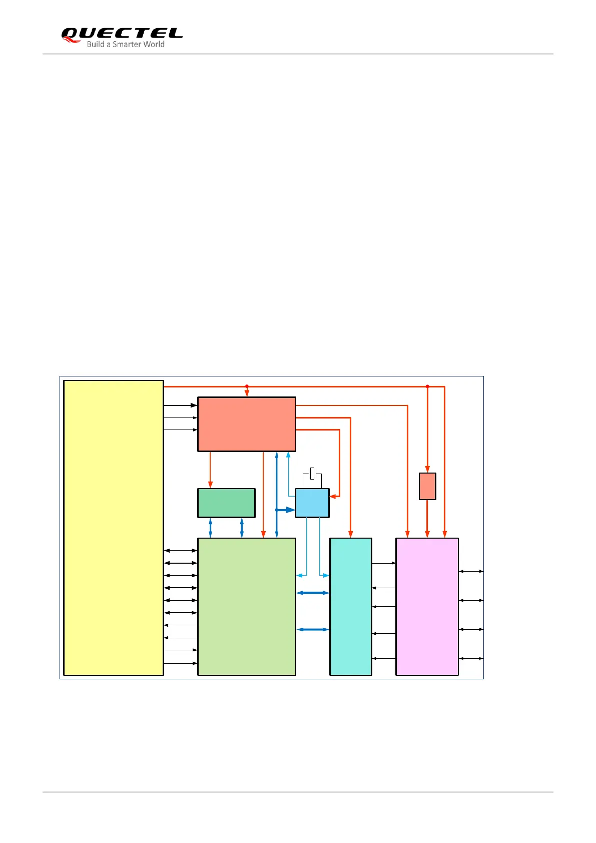
2.4. Functional Diagram
The following figure shows the functional diagram of RM500Q-GL.
Power management
Baseband
LPDDR4X SDRAM + NAND Flash
Radio frequency
M.2 Key-B interface
ANT0
ANT3
ANT2_GNSSL1
38.4MHz XO
Qlink
Control
Tx
PRx
DRx
PCI Express M.2 Key-B Interface
FULL_CARD_POWER_OFF#
W_DISABLE2#
USB 2.0 & USB 3.1
(U)SIM1
WWAN_LED#
WAKE_ON_WAN#
RFFE
W_DISABLE1#
GPIOs
ANT1
PCIe 3.0 × 1
(U)SIM2
GND
RESET#
VCC
SPMI
Clock IC
BB_CLK 19.2MHz
RF_CLK 38.4MHz
EBI1
EBI2
32.768kHz
PMIC
MCP
NAND 4Gb x 8
LPDDR4X 4Gb x 16
Baseband
Sub-6 GHz
Transceiver
Tx/Rx Blocks
ET
Figure 1: Functional Block Diagram

Table of Contents

Other manuals for Quectel 5G Series

Questions and Answers:

Question and Answer IconNeed help?

Do you have a question about the Quectel 5G Series and is the answer not in the manual?

Quectel 5G Series Specifications

General IconGeneral
BrandQuectel
Model5G Series
CategoryControl Unit
LanguageEnglish

Related product manuals