EasyManuals Logo

Quectel 5G Series Hardware Design

Quectel 5G Series
86 pages
To Next Page IconTo Next Page
To Previous Page IconTo Previous Page
Page #47 background imageLoading...
Page #47 background image
5G Module Series
RM500Q-GL Hardware Design
RM500Q-GL_Hardware_Design 46 / 85
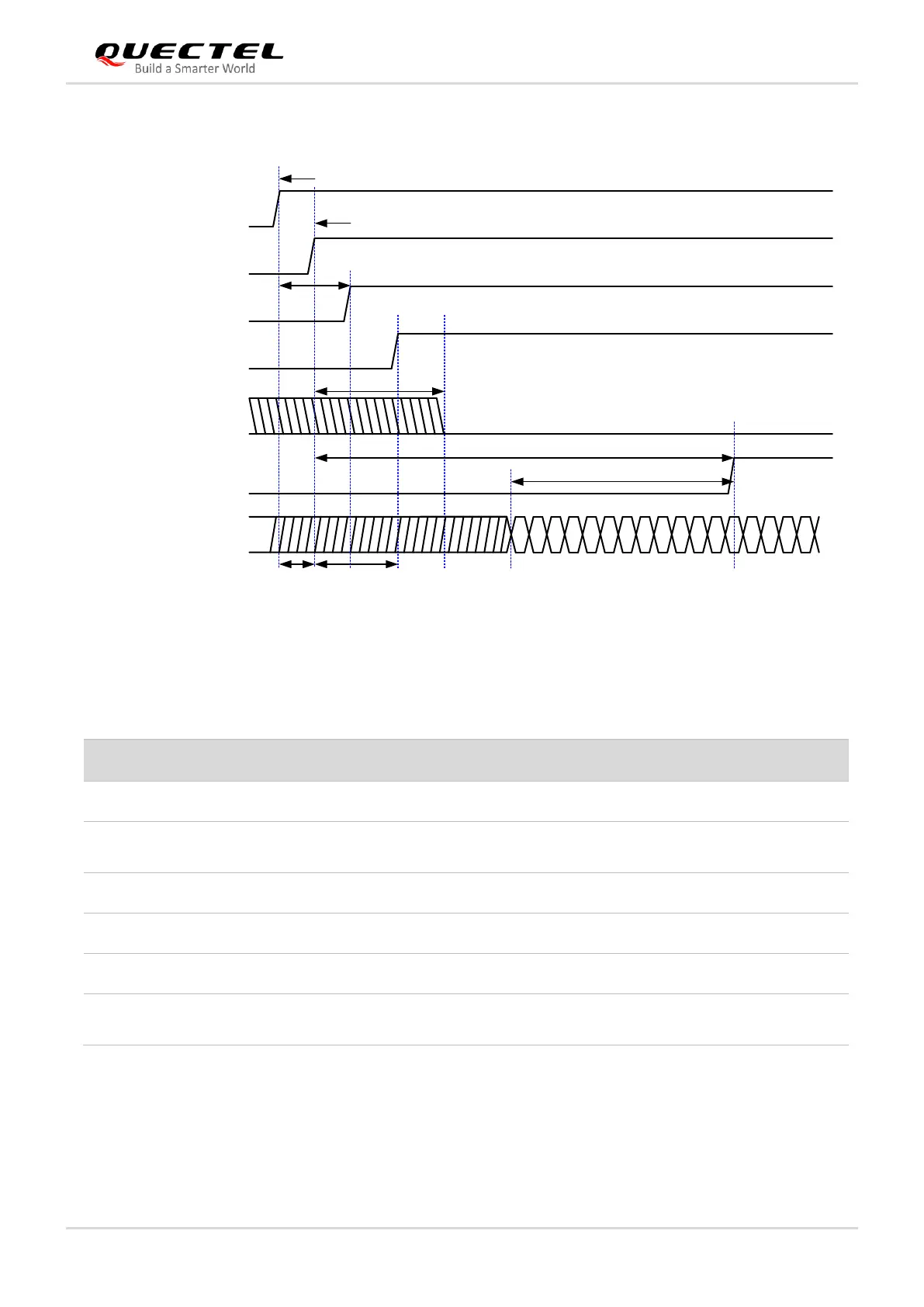
The following figure and table are PCIe turn-on timing and variables of the module.
T
FCPO#-CLKREQ#
> 90 ms
PCIE_CLKREQ_N
PCIE_RST_N
PCIE_REFCLK
T
power-on
T
turn-on
VCC
FCPO#
Module power-on or insertion detection
RESET#
RFFE_VIO_1V8
System turn-on and booting
V
IH
1.19 V
1.8 V
3.7 V
1.8 V
T
FCPO#-PERST#
> 100 ms
T
PERST#-CLK
> 100 us
T
VCC-RST#
Figure 21: PCIe Power-on Timing of the Module
Table 18: PCIe Turn-on Timing of the Module
Symbol
Min.
Typ.
Max.
Comment
T
power-on
0 ms
20 ms
-
Module power-on time depending on the host.
T
VCC-RST#
-
33 ms
-
Time period between module power-on and
RESET# being driven HIGH.
T
turn-on
68 ms
-
-
Module system turn on time.
tFCPO#-CLKREQ#
90 ms
100 ms-
-
PCIe clock request.
tFCPO#-PERST
100 ms
-
-
PCIe reset.
T
PERST#-CLK
100 μs
-
-
The time period during which REFCLK is stable
before PERST# is inactive.

Table of Contents

Other manuals for Quectel 5G Series

Questions and Answers:

Question and Answer IconNeed help?

Do you have a question about the Quectel 5G Series and is the answer not in the manual?

Quectel 5G Series Specifications

General IconGeneral
BrandQuectel
Model5G Series
CategoryControl Unit
LanguageEnglish

Related product manuals