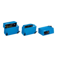
CDB620-001
PNP sensor 3
V
S
GND
12 SGND
6 Shield
11
U
IN
*
A
Out
U
IN
*
GND
S3
Trigger sensor 1
ON
OFF
S3 : SGND-GND
V
S ext
Shield
U
IN
*
CDB620-001
12 SGND
6 Shield
11
U
IN
*
A
GND
S3
ON
OFF
S3 : SGND-GND
Shield
1
V
S ext
GND
A
12
2
Sens B
Sens B
2
2
4
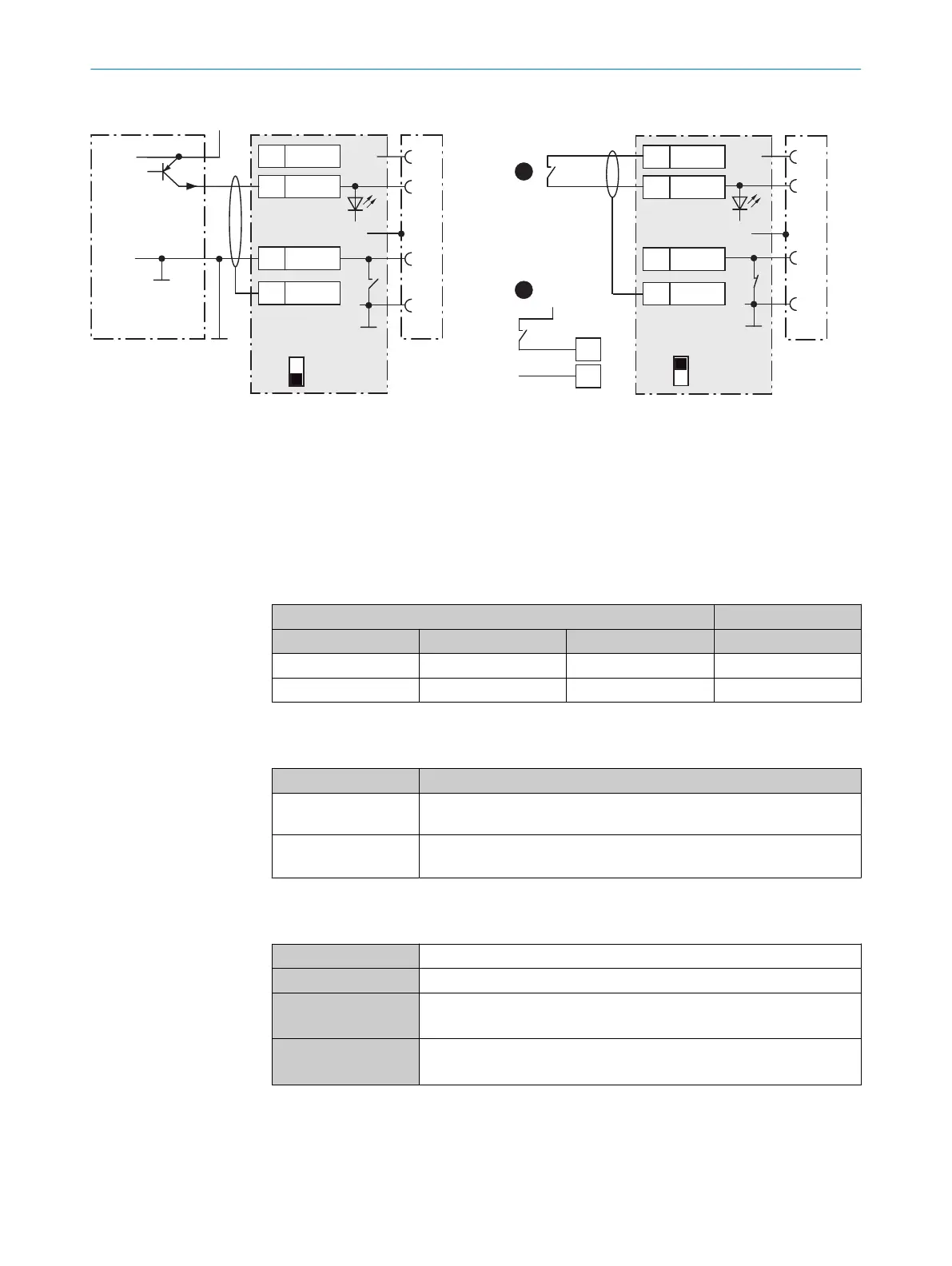
Figure 46: Left: Trigger sensor connected potential-free and supplied with power externally. Right: alternative switch,
!
supplied with power by connection module CDB620-001 or
"
connected volt-free and supplied with power externally. Now
select switch setting S3 as shown in the left figure.
1
Trigger sensor, e.g. for read cycle generation
2
External supply voltage V
S ext
3
PNP sensor
4
Supply voltage V
S
Table 24: Assignment of placeholders to the digital inputs
CDB620-001 Device
Terminal A Signal B Pin C Sensor D
10 Sens 1 14 1
13 Sens 2 4 2
Function of switch S3
Table 25: Switch S3: SGND - GND
Switch setting Function
ON GND of the trigger sensor is connected with GND of CDB620-001 and
GND of the device
OFF Trigger sensor is connected volt-free at CDB620-001 and the device.
Common, isolated reference potential of all digital inputs is SGND.
Characteristic data of the digital inputs
Table 26: Characteristic data of the digital inputs “Sensor 1” and “Sensor 2”
Type Switching
Switching behavior Power to the input starts the assigned function, e.g. start read cycle.
Properties
•
Opto-decoupled, reverse polarity protected
•
Can be wired with PNP output of a trigger sensor
Electrical values Low: V
in
1)
≤ 2 V; I
in
2)
≤ 0.3 mA
High: 6 V ≤ V
in
≤ 30 V; 0.7 mA ≤ I
in
≤ 5 mA
1)
Input Voltage
2)
Input current
14 ANNEX
82
O P E R A T I N G I N S T R U C T I O N S | CLV61x 8017840/19OF/2021-10-28 | SICK
Subject to change without notice
 Loading...