8.1 Structure of the Memory Area
The memory of the CPU 948 is essentially divided into the following
areas:
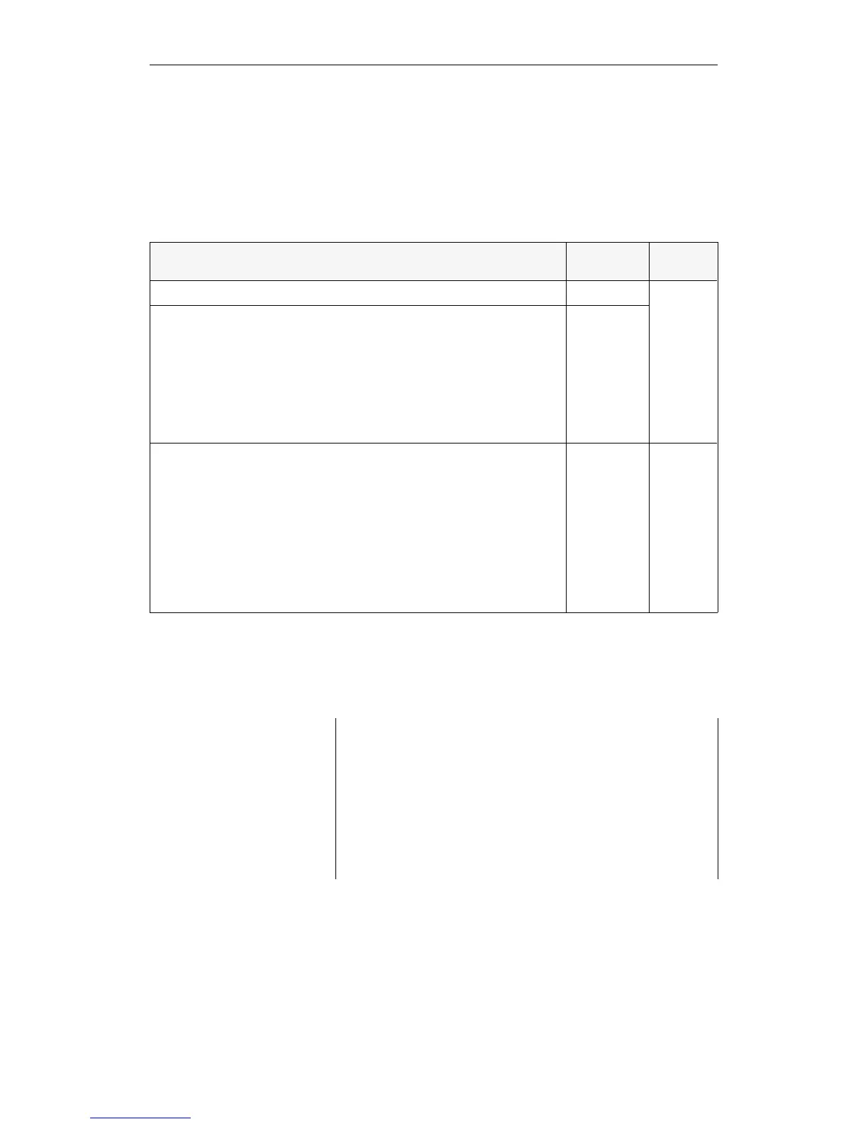
Memory area Data width Location
User memory for: OBs, FBs, FXs, PBs, SBs, DBs, DXs 16 bits
CPU
internal
Serial communications interface area: RI, RJ
System area: RS, RT
Timers: T
Counters: C
Flags: F
Flags: S
Process image (PI) inputs/
outputs: PII, PIQ
16 bits
16 bits
16 bits
16 bits
8 bits
8 bits
1)
8 bits
Peripheral area,
divided into:
"P" peripherals
"O" peripherals
Interprocessor communication flags
Coordinator (COR) (semaphore, ...)
Dual-port RAM pages (CP, IP, COR 923C)
Distributed peripherals
Hardware registers
8 bits
8 bits
8 bits
8 bits
8/16 bits
8 bits
8/16 bits
On the
S5 bus
1)
S flags occupy 8 bits in the 16-bit area. The high byte is undefined.
The next section lists the addresses of the memory areas shown.
Note
When using STEP 5, you should not access a memory register
within an operand area (e.g., flags) directly via the absolute
address of the memory register. This can result in undesirable
operating statuses. Access it only relative to the base address of its
operand area.
Direct access to the areas I, Q and F result in ’FFH’ in the high
byte and the data in the low byte. For direct access to S flags, the
high byte is undefined!
Table 8-1 Structure of the memory area
Structure of the Memory Area
CPU 948 Programming Guide
8 - 4 C79000-G8576-C848-04