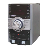
HCD-MD333
– 39 – – 40 –
THIS NOTE IS COMMON FOR PRINTED WIRING
BOARDS AND SCHEMATIC DIAGRAMS.
(In addition to this, the necessary note is printed
in each block.)
For schematic diagrams.
Note:
• All capacitors are in µF unless otherwise noted. pF: µµF
50 WV or less are not indicated except for electrolytics
and tantalums.
• All resistors are in Ω and
1
/4
W or less unless otherwise
specified.
•
¢
: internal component.
• 2 : nonflammable resistor.
• 1 : fusible resistor.
•
M
: Switch with sliding contact indicated by hatched
lines shows shorting type.
• C : panel designation.
For printed wiring boards.
Note:
• X : parts extracted from the component side
•
®
: Through hole.
•
¢
: internal component.
• b : Pattern from the side which enables seeing.
(The other layers' patterns are not indicated.)
• U : B+ Line.
• V : B– Line.
• H : adjustment for repair.
Signal path.
F : FM
E : PB (MD)
m : PB (TAPE)
n : REC
J : CD
c : digital out
• Abbreviation
CND : Canadian model.
EE : East European model.
SP : Singapore model.
MY : Malaysia model.
JE : Tourist model.
HK : Hong Kong model.
AR : Argentine model.
AUS : Australian model.
IC103 3 (MDP) (PALY Mode)
1
2
3
4
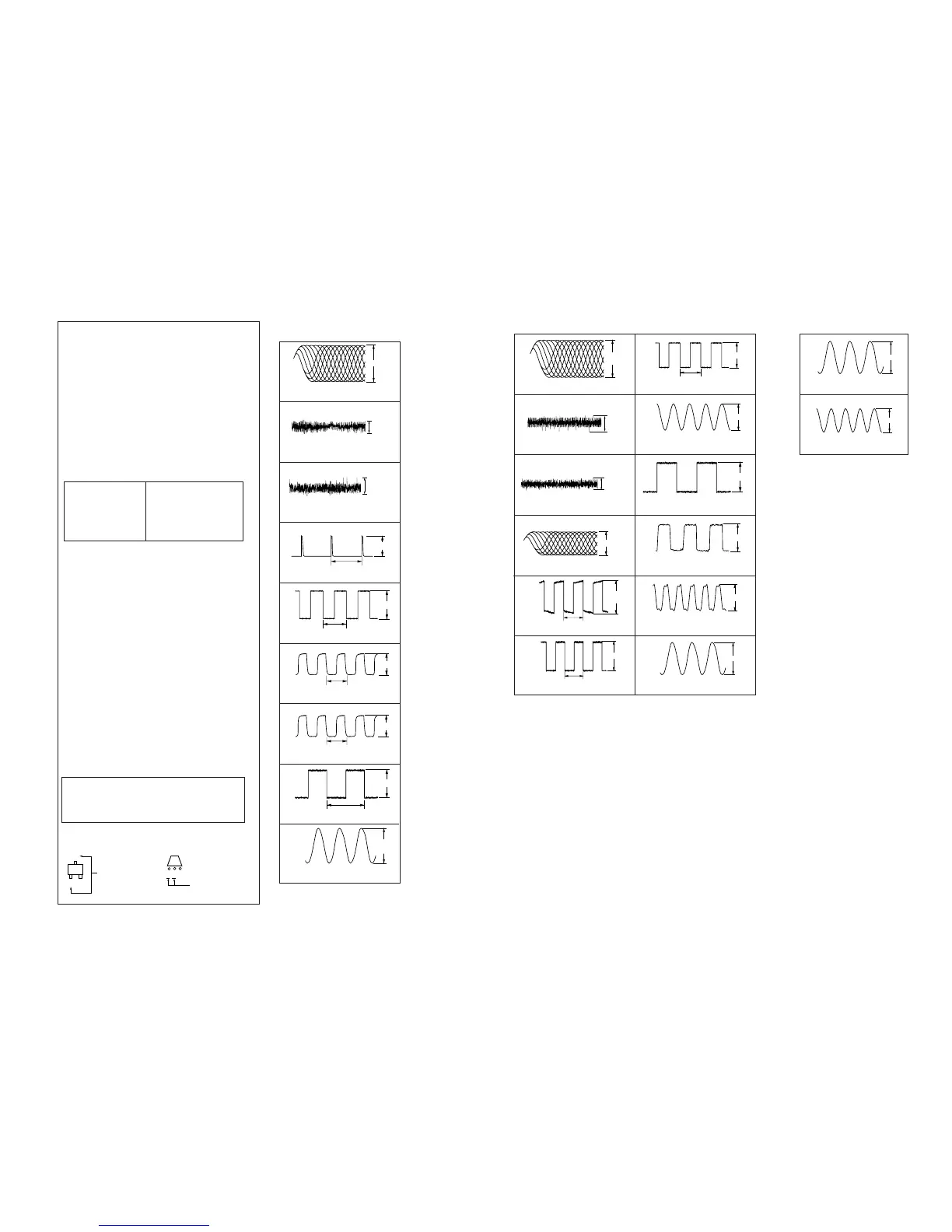
WAVEFORMS
– CD SECTION –
IC101 #¡ (RFO) (PLAY Mode)
500 mV/DIV, 500 ns/DIV
IC101 $¢ (TEI) (PLAY Mode)
50 mV/DIV, 1 µs/DIV
IC101 2 (FEI) (PLAY Mode)
50 mV/DIV, 1 µs/DIV
• Indication of transistor
1
2
3
4
IC101 8, 9 (E, F) (PLAY Mode)
IC101 #• (RF) (PLAY Mode)
5
6
7
8
9
!º
IC121 @§ (XBCK)
IC121 @∞ (LRCK)
!¡
!™
IC501 1, 2 (I.J) (PLAY Mode)
IC101 4 (A) (PLAY Mode)
IC152 #™ (CAPA–) (PLAY Mode)
IC152 #™ (CAPA+) (PLAY Mode)
IC121 (º (FS4)
IC121 !¶ (OSCI)
IC121 @¶ (FS256)
IC316 !£ (XOUT)
– MD SECTION –
Caution:
Pattern face side: Parts on the pattern face side seen from the
(Side B) pattern face are indicated.
Parts face side: Parts on the parts face side seen from the
(Side A) parts face are indicated.
C
These are omitted
EB
Q
C
These are omitted
EB
Note:
The components identi-
fied by mark ! or dotted
line with mark ! are criti-
cal for safety.
Replace only with part
number specified.
Note:
Les composants identifiés par
une marque ! sont critiques
pour la sécurité.
Ne les remplacer que par une
piéce portant le numéro
spécifié.
IC103 @º (LRCK)
5
6
7
8
IC103 @• (RFCK)
IC103 @∞ (XPCK)
IC103 @™ (BCLK)
IC104 6 (XTO)
9
1
2
– MAIN SECTION –
IC601 !¡ (XI)
IC601 !¢ (XI)
1.3 ± 0.3 Vp-p
Approx.
100 mVp-p
Approx.
150 mVp-p
2.6 Vp-p
7.6 µs
5.1 Vp-p
136 µs
5.3 Vp-p
14 ns
5 Vp-p
474 ns
5.1 Vp-p
22.8 µs
4.6 Vp-p
16.9344 MHz
Approx.
500 mVp-p
Approx.
200 mVp-p
Approx.
150 mVp-p
 Loading...