Do you have a question about the Sony HCD-MD333 - Hi Fi Cd/minidisc Component and is the answer not in the manual?
| Brand | Sony |
|---|---|
| Model | HCD-MD333 - Hi Fi Cd/minidisc Component |
| Category | Car Receiver |
| Language | English |
Lists the various model designations supported by this service manual.
Details the power output and total harmonic distortion specifications for the amplifier section.
Covers specifications for CD, MD, Tuner sections, and general system parameters.
Explains the system malfunction display codes and their meanings for user reference.
Step-by-step guide to access the error history display mode for servicing.
Describes the various data items displayed within the error history mode.
Lists error codes with their corresponding details and potential causes.
Warnings regarding laser radiation exposure and necessary precautions.
Guidelines for handling chip components and flexible circuit boards during repair.
Highlights critical components that must be replaced with specified parts.
Procedure and limits for checking AC leakage from exposed metal parts.
Precautions for handling the optical pick-up block and base unit, including ESD.
Instructions on how to remove the disc table from the unit.
Notes on checking laser diode emission and safety precautions.
Procedure to prevent scratches on the front panel during window removal.
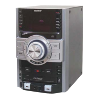
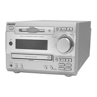
Diagram identifying the main controls and indicators on the front panel.
Detailed list and numbering of all parts and controls on the front panel.
Step-by-step instructions for setting the system's clock time.
Guidance on correcting errors and modifying the preset time settings.
Steps for disassembling and removing the main case of the unit.
Procedure to detach the front panel and MD mechanism deck assembly.
Instructions for removing the back panel and jack board.
Procedure for disassembling and removing the MD mechanism deck.
Steps for disassembling and removing the CD mechanism deck.
Procedure for detaching the BD (MD) board from the unit.
Instructions on how to remove the disc table assembly.
Procedure for disassembling and removing the sub chassis.
Steps for disassembling and removing the optical pick-up unit.
Procedure for removing the over write head assembly.
Steps for disassembling and removing the slider complete assembly.
Procedure for disassembling and removing the shutter assembly.
Procedure to change AM/LW tuner channel step intervals.
How to activate all-lit and key check modes for LEDs and indicators.
Procedure for checking the sub clock signal using an oscilloscope.
Safety and usage guidelines for operating the system in test mode.
Instructions on how to enter and exit the various test modes.
Describes the basic operation of controls within the test mode environment.
How to operate the continuous playback mode for testing purposes.
How to operate the continuous recording mode for testing purposes.
Description of the non-volatile memory read/write mode.
Explains the functions of various buttons used within test modes.
Explains the display sequence and meanings of various indicators in test mode.
Describes the sequence of operations performed in the aging mode.
Lists error messages and main causes that stop the aging process.
Safety precautions for checking laser diode emission and using optical pick-ups.
General precautions, parts replacement notes, and required tools for adjustments.
Procedure for creating a continuously recorded disc for adjustments.
Procedure to adjust and save temperature compensation offset data.
Procedure to adjust laser power levels for optimal performance.
Procedure to adjust traverse waveforms for CD and MD discs.
Procedure to adjust focus bias for optimal performance.
Procedures for checking CD and MO error rates.
Procedure to check focus bias tolerance levels.
Diagrams showing test points and connections on the BD (MD) board.
Details S-curve check, focus bias, and RF level checks for the CD section.
Identifies the physical locations of all circuit boards within the unit.
Provides a block diagram illustrating the CD section's signal flow and components.
Provides a block diagram illustrating the MD section's signal flow and components.
Provides block diagrams for the main section's signal flow and components.
Displays typical waveforms for key ICs in the CD section.
Displays typical waveforms for key ICs in the MD section.
Displays typical waveforms for key ICs in the Main section.
Detailed circuit diagram for the CD section.
First part of the detailed circuit diagram for the MD section.
Second part of the detailed circuit diagram for the MD section.
Third part of the detailed circuit diagram for the MD section.
Shows component layout for the MD section printed wiring boards.
First part of the detailed circuit diagram for the Main section.
Second and third parts of the detailed circuit diagram for the Main section.
Shows component layout for the Main section printed wiring board.
Detailed circuit diagram for the Audio section.
Shows component layout for the Audio section printed wiring board.
Detailed circuit diagram for the Panel section.
Shows component layout for the Panel section printed wiring board.
Detailed circuit diagram for the Jack section.
Shows component layout for the Jack section printed wiring board.
Detailed circuit diagrams for the ST terminal and loading sections.
Shows component layout for the ST terminal and loading boards.
Detailed circuit diagram for the transformer section.
Shows component layout for the transformer section board.
Detailed circuit diagram for the power amplifier section.
Shows component layout for the power amplifier board.
Block diagrams illustrating the ICs used in the CD section.
Pinout and function details for IC101, the RF amplifier.
Pinout and function details for IC121, the digital signal processor.
Pinout and function details for IC316, the MD system control IC.
Pinout and function details for IC601, the master control IC.
Exploded view illustrating the assembly of the front panel components.
Exploded view showing the chassis, main boards, and transformer assembly.
Exploded view of the MD mechanism deck assembly (Part 1).
Exploded view of the MD mechanism deck assembly (Part 2).
Exploded view of the CD mechanism deck assembly (Part 1).
Exploded view of the CD mechanism deck assembly (Part 2).
List of electrical components for the Audio section.
Summary of parts that have been changed in revisions.
Details revision 1.1, including correction of exploded views.
Details revision 1.0, marking the initial release of the manual.