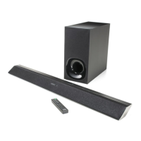
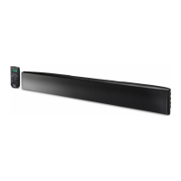
SA-WS350/WSD35
20
Sony CONFIDENTIAL
For Authorized Servicer
THIS NOTE IS COMMON FOR PRINTED WIRING BOARDS AND SCHEMATIC DIAGRAMS.
(In addition to this, the necessary note is printed in each block.)
For Printed Wiring Boards.
Note:
• : Pattern from the side which enables seeing.
(The other layers’ patterns are not indicated.)
Caution:
Pattern face side:
(Conductor Side)
Parts face side:
(Component Side)
Parts on the pattern face side seen
from the pattern face are indicated.
Parts on the parts face side seen from
the parts face are indicated.
Caution:
Pattern face side:
(SIDE B)
Parts face side:
(SIDE A)
Parts on the pattern face side seen
from the pattern face are indicated.
Parts on the parts face side seen from
the parts face are indicated.
For Schematic Diagrams.
Note:
• All capacitors are in μF unless otherwise noted. (p: pF)
50 WV or less are not indicated except for electrolytics
and tantalums.
• All resistors are in Ω and 1/4 W or less unless otherwise
specifi ed.
Note:
The components identi-
fi ed by mark 0 or dotted
line with mark 0 are criti-
cal for safety.
Replace only with part
number specifi ed.
Note:
Les composants identifi és
par une marque 0 sont
critiques pour la sécurité.
Ne les remplacer que par
une pièce portant le nu-
méro spécifi é.
Note 1: When boards installed in this unit are defective, boards will be
replaced.
Individual electrical parts that mounted on the board cannot be
replaced.
When each board is defective, replace each complete mounted
board individually.
Note 2: When the complete MAIN board is replaced, be sure to refer to
“WIRELESS CONNECTION (LINK) WORK OF THE BAR
SPEAKER AND THE SUBWOOFER” on page 6.
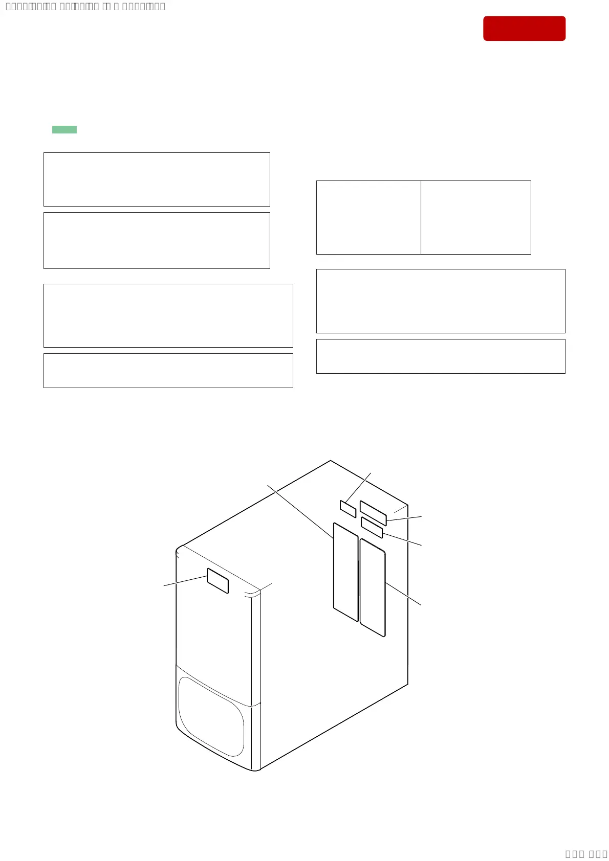
• Circuit Boards Location
MAIN board
KEY board
MINI JACK board
LED board
POWER board
BT module (SW)
(BT1)
SYSSET
2019/02/1301:37:00(GMT+09:00)