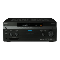
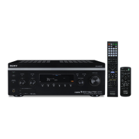
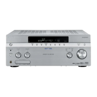
90
STR-DA5000ES
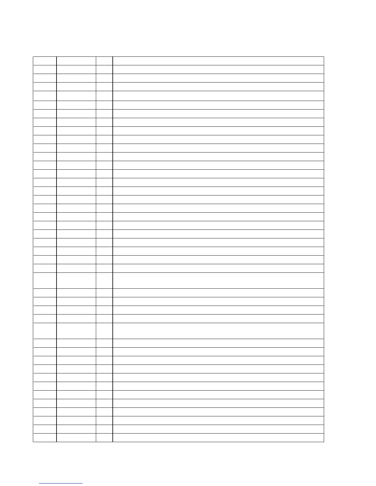
6-59. IC PIN FUNCTION DESCRIPTION
• DIGITAL BOARD IC2121 LC89056W-E (DIGITAL AUDIO INTERFACE RECEIVER)
Pin No. Pin Name I/O Description
1 DISEL
I
Selection signal input terminal of data input terminal Fixed at “L” in this set
2
DOUT
O
Digital data output to the external output terminal Not used
3
DIN0
I
Digital data input from the external input terminal
4, 5
DIN1,DIN2
I
Digital data input from the external input terminal Fixed at “L” in this set
6
D. GND
—
Ground terminal (for digital)
7
DVDD
—
Power supply terminal (+3.3V) (for digital)
8
R
I
Input terminal for VCO gain control
9
VIN
I
Input terminal for VCO free-run frequency setting
10
LPF
O
PLL loop filter setting terminal
11
AVDD
—
Power supply terminal (+3.3V) (for analog)
12
AGND
—
Ground terminal (for analog)
13
CKOUT
O
Audio clock signal output to the selector
14
BCK
O
Bit clock signal (2.8224 MHz) output to the digital signal processor and A/D converter
15 LRCK
O
L/R sampling clock signal (44.1 kHz) output to the digital signal processor and A/D converter
16 DATAO
O
Audio serial data output to the digital signal processor and main system controller
17 XSTATE
O
Source clock selection monitor output to the main system controller
18 DGND
—
Ground terminal (for digital)
19 DVDD
—
Power supply terminal (+3.3V) (for digital)
20 XMCK
O
System clock signal (12.288 MHz) output to the A/D converter
21 XOUT
O
System clock output terminal (12.288 MHz) Not used
22 XIN
I
System clock input terminal (12.288 MHz)
23 EMPHA
O
Channel status emphasis information output terminal Not used
24 AUDIO
O
Channel status bit 1 output to the digital signal processor
25
CSFLAG
O
Channel status head 40 bit renewal flag output terminal Not used
26 to 29
F0/P0/C0 to
F3/P3/C3
O
Output terminal of input frequency calculation result Not used
30 DVDD
—
Power supply terminal (+3.3V) (for digital)
31 DGND
—
Ground terminal (for digital)
32 AUTO
O
Not used
33 BPSYNC
O
Non-PCM burst preamble sync signal output terminal Not used
34
ERROR
O
PLL lock error signal and data error flag output to the digital signal processor and main system
controller
35 DO
O
Read data output to the main system controller
36 DI
I
Write data input from the main system controller
37 CE
I
Chip enable signal input from the main system controller
38 CLK
I
Clock signal input from the main system controller
39 XSEL
I
Selection signal input terminal of crystal oscillator frequency Fixed at “H” in this set
40, 41
MODE0, MODE1
I
Mode setting terminal Fixed at “L” in this set
42 DGND
—
Ground terminal (for digital)
43 DVDD
—
Power supply terminal (+3.3V) (for digital)
44, 45
DOSEL0, DOSEL1 I
Output data format selection signal input terminal Fixed at “L” in this set
46 CKSEL0
I
Output clock selection signal input terminal Fixed at “L” in this set
47 CKSEL1
I
Output clock selection signal input from the main system controller
48 XMODE
I
System reset signal input from the main system controller “L”: reset