111/317
5-Peripherals
The change of the state of an output pin;
The reset of the free-running counter (only in PWM mode).
The PWM mode will be studied later.
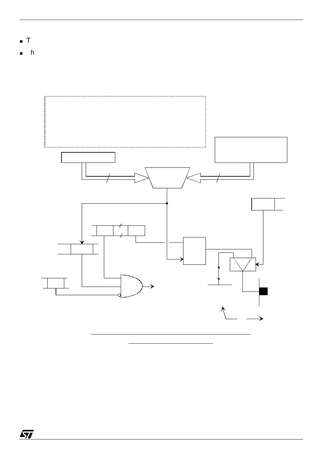
The block diagram of one of the compare circuits is the following:
05-comp
Output compare and corresponding interrupt mechanism:
diagram for channel 1, timer A
I
Condition code
register (CCR)
OCIE
Timer A control
register 1 (TACR1)
Output compare 1
interrupt to
the core
OLVL1
Free running counter
16 bit output compare register
TAOC1HR, TAOC1LR
(Read / write registers)
OCF1 : Output compare flag 1 bit (bit 6 of TASR)
OCIE : Output compare interrupt enable bit (bit 6 of TACR1)
OLVL1 : Output level 1 bit (bit 0 of TACR1)
OC1E : Output compare 1 enable bit (bit 7 of TACR2)
reset : general purpose I/O pin
set : timer A output compare 1 pin (OCMP1)
I : Global interrupt enable bit (bit 3 of CCR)
16
16
Compare
OCF1*
Timer A status
register (TASR)
Clk
Output
compare 1
pin for
timer A
General
purpose
I/O channel
OC1E
Timer A control
register 2 (TACR2)
or
*cleared by a TASR read access
followed by an access to TAOC1LR
latch
10