DocID15067 Rev 3 41/49
AN2834 How to get the best ADC accuracy
48
3.4.3 Minimizing additional errors
Workaround for high impedance sources
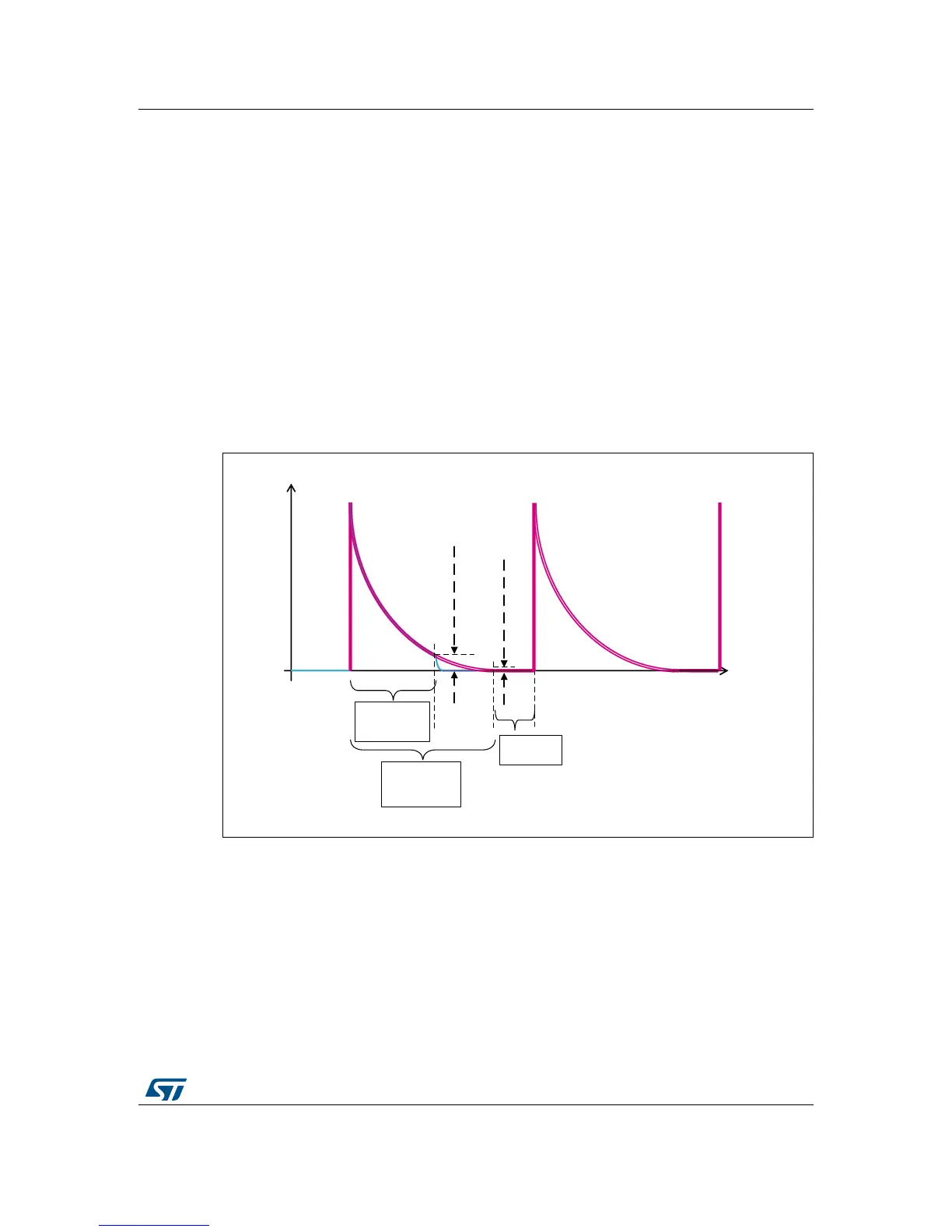
To solve the additional error problem, the sampling time (T
S
) can be increased by
configuring ADC settings in MCU firmware, so that the C
sh
charge is discharged through the
source impedance R
in
. The time constant (R
in
x C
sh
) is the reference for choosing the
sampling time. To calculate the sampling time cycles, use this formula (for a maximum error
of 1/2 LSB, see also Section 3.2.6):
The ADC clock (f
ADC
) is another important factor, since slowing down the ADC clock
increases the sampling time.
Figure 35. Effect of sampling time extension
If the maximum register value of the sampling time (T
S
) setting is reached and the problem
is still present, you need a more complex solution which is applicable also for
measurements of source with extra high internal impedance (see Section : Workaround for
extra high impedance sources).
Note that for this application you
must take into account not only the internal sampling
capacitance, but also any external parasitic capacitance (in parallel to C
ext
), such as pin
capacitance or PCB path capacitance.
Do not add any external capacitor (C
ext
) to the input pin when applying this above
workaround. Its capacity will increase the timing constant (R
in
x C
sh
|| C
ext
) and the problem
will remain.

 Loading...


