How to get the best ADC accuracy AN2834
32/49 DocID15067 Rev 3
3.2.11 EMI-induced noise reduction
You can reduce EMI noise using proper shielding and layout techniques. The possible
sources of emission must be physically separated from the receptors. They can be
separated electrically by proper grounding and shielding.
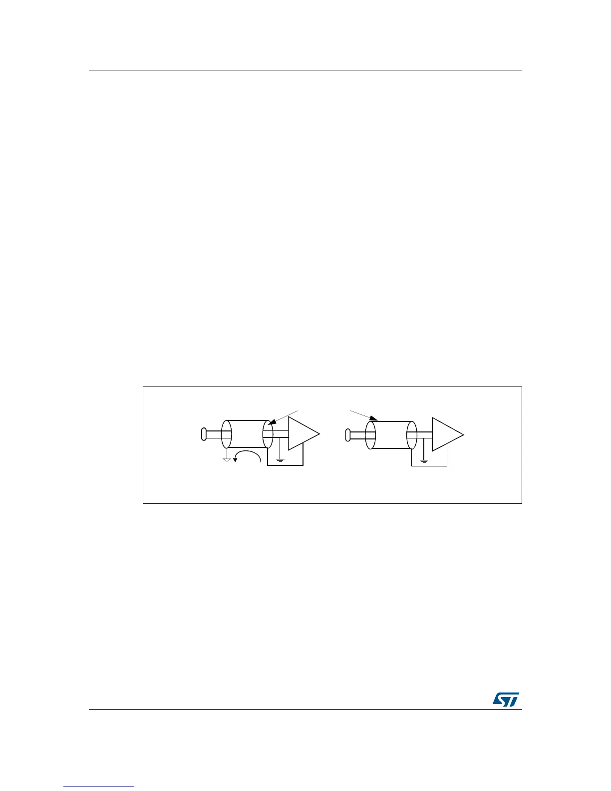
Shielding technique
Placing ground tracks alongside sensitive analog signals provides shielding on the PCB.
The other side of the two-layer PCB should also have a ground plane. This prevents
interference and I/O crosstalk affecting the signal (see Figure 28).
Signals coming from distant locations (such as sensors) shou
ld be connected to the PCB
using shielded cable. Care should be taken to minimize the length of the paths of these
types of signal on the PCB.
The shield should not be used to carry the ground reference from the sensor or analog
sour
ce to the microcontroller. A separate wire should be used as ground. The shield should
be grounded at only one place near the receiver such as the analog ground of the
microcontroller. Grounding the shield at both ends (source and receiver) might lead to the
creation of ground loops, with the result of current flowing through the shield. In this case,
the shield acts like an antenna and the purpose of the shielding is lost.
The shielding concept also applies
to grounding the c
hassis of the application if it is metallic.
And it also helps remove EMI and EMC interference. In this case the mains earth ground is
used to shield the chassis. Similarly DC ground can be used for shielding in case of the
earth ground not being available.
Figure 28. Shielding technique

 Loading...


