DocID15067 Rev 3 45/49
AN2834 How to get the best ADC accuracy
48
3.4.4 Source of described problem - ADC design
The following sections list some possible causes for the charging of the internal sampling
capacitor C
sh
. This is not an exhaustive list; only the main possible sources of the ADC
design are mentioned.
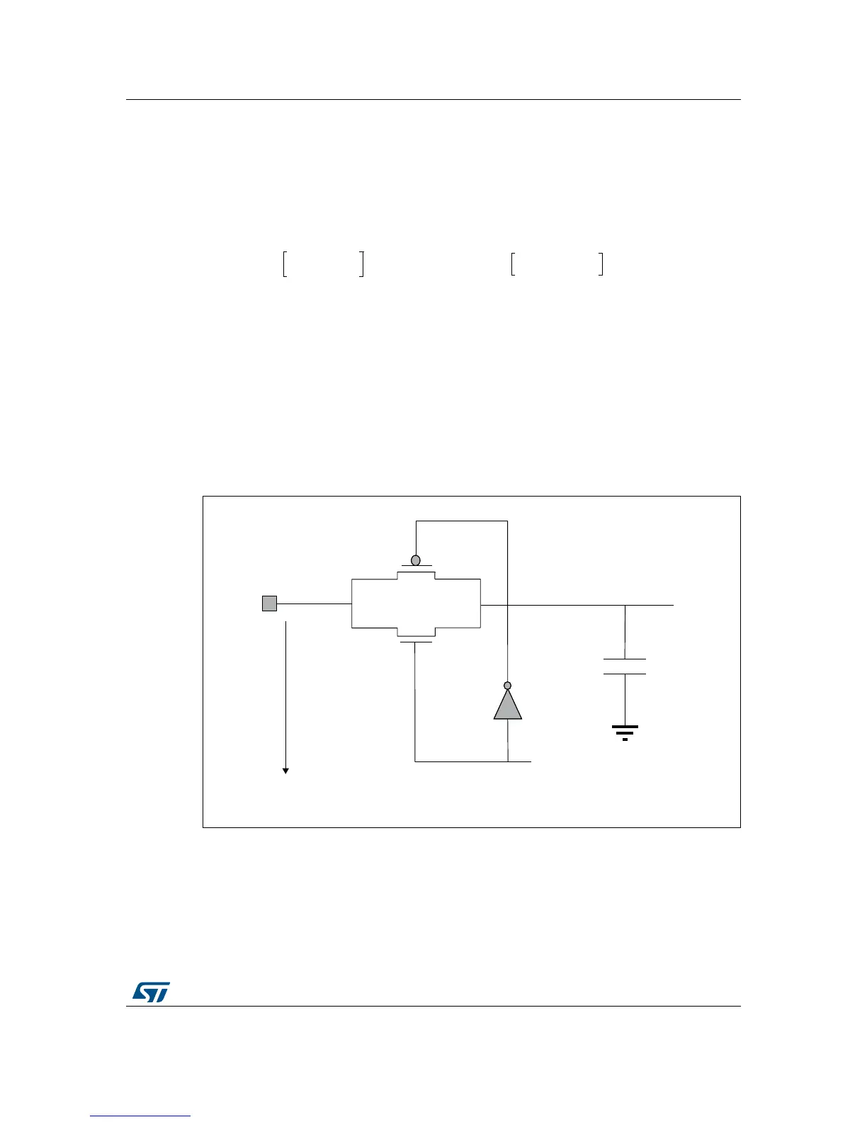
Parasitic switch capacitance effect
The sampling switch inside ADC sampling circuit (see Figure 33) is not ideal. In reality the
sample and hold switch (S
1
) is designed as 2 transistors (PMOS and NMOS, see
Figure 37):
Figure 37. Implementation of sampling switch
The switch is controlled by the gate voltages of tran
sistors (inverted signal on PMOS
transistor). This design is a standard bidirectional switch (for rail to rail range of input U
in
voltages). Both transistors have parasitic capacitances between gate and source.
If those capacitances are charged (close to the switch),
then their charge can be transferred
to the sampling capacitor (see Figure 38).
U
max
= 4096 LSB ..... ADC property
U
lsb
= 0.5 LSB ..... required precision

 Loading...


