DocID15067 Rev 3 33/49
AN2834 How to get the best ADC accuracy
48
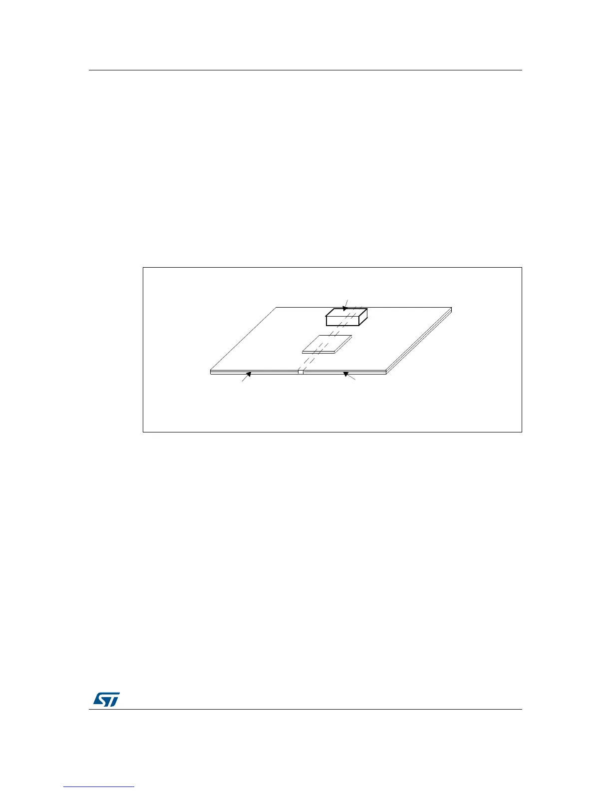
3.2.12 PCB layout recommendations
Separating the analog and digital layouts
It is recommended to separate the analog and digital circuitry on the PCB (see Figure 29).
This also avoids tracks crossing each other. The tracks carrying digital signals may
intr
oduce high-frequency noise in analog signals because of coupling.
The digital signals produce high-frequency noise because of fast switching.
Coupling of a capacitive nature is formed due to the metal connections (tracks) separated
by
the dielectric provided by the PCB base (glass, ceramic or plastic).
It is recommended to use different planes for analog
and digital grounds. If there is a lot of
analog circuitry then an analog ground plane is recommended. The analog ground must be
placed below the analog circuitry.
Figure 29. Separating the analog and digital layouts
Separating the analog- and digital-circuit power supplies
It is desirable to have separate analog and digital power supplies in cases where there is a
lot of analog and digital circuits external to the microcontroller (see Figure 30). Depending
on the STM32 package, different analog and digi
tal power supply and ground pins are
available. The V
DDA
/V
REF+
and V
DD
pins can be powered from separate power supplies.
If you use a switching-type power supply for the digi
tal circuitry, you should use a separate
linear supply for the analog circuit. Also, if you expect a lot of noise on the DC power supply
due to I/O switching etc., it is preferable to use a separate supply for the analog circuit.

 Loading...


