How to get the best ADC accuracy AN2834
28/49 DocID15067 Rev 3
3.2.6 Analog source resistance calculation
Let us assume that the maximum error allowed is equal to 1/2 LSB. We will calculate the
maximum source resistance allowed.
V
c
is the voltage across the internal C
ADC
capacitor (refer to Figure 15).
Then we have:
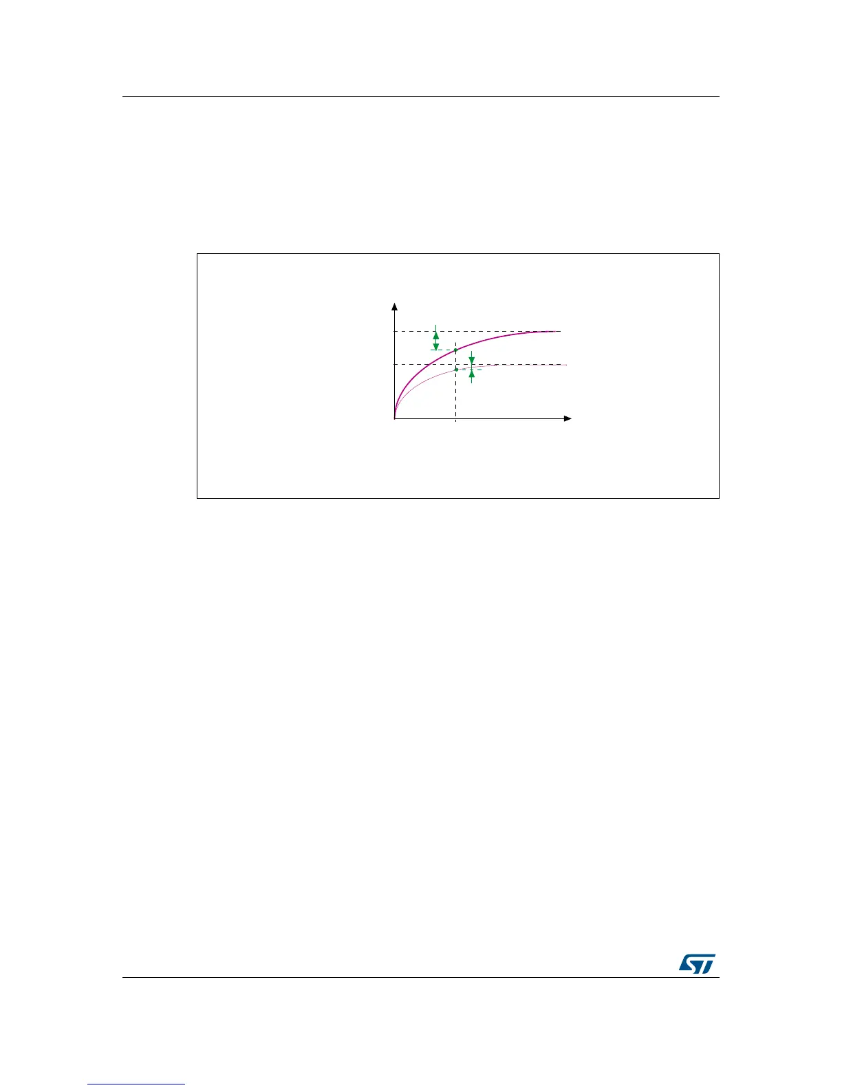
Figure 25. Worst case error: V
AIN
= V
REF+
Let t
s
be the sampling time.
t
s
= T
S
/f
ADC
, where T
s
is the sampling time evaluated by cycles (1)
For a given t
s
, the error corresponding to V
AIN
= V
REF+
is greater than the error
corresponding to V
AIN
< V
REF+
because the C
ADC
capacitor takes more time to charge from
0 V to V
AIN
when V
AIN
= V
REF+
than it takes when V
AIN
< V
REF+
(refer to Figure 25). So
V
AIN
= V
REF+
is the worst case to be taken into account in the demonstration of the
maximum source resistance.
Error V
REF+
V
REF+
1e
t
s
R
max
C
ADC
--------------------------------–
–
⎝⎠
⎜⎟
⎜⎟
⎜⎟
⎜⎟
⎛⎞
–
1
2
---
V
REF+
2
N
------------------ -
⋅==
where:
R
max
= (R
AIN
+ R
ADC
)max(2)
N is the ADC resolution (in our case N = 12)
This gives:
e
t
s
R
max
C
ADC
--------------------------------
–
1
2
N1+
-----------=
R
max
t
s
C
ADC
2
N1+
()ln⋅
-------------------------------------------- -
=
DLE
9
$,1
9
5()
9
$,1
9
5()
(UURU9
$,1
9
5()
!(UURU9
$,1
9
5()
9
9
F
W
(UURU9
$,1
9
5()
W
V
(UURU9
$,1
9
5()

 Loading...


