How to get the best ADC accuracy AN2834
40/49 DocID15067 Rev 3
3.4.2 Explanation of the behavior
The explanation of this additional pin noise and additional measurement error (in case a
signal source with high internal impedance is used) comes from the internal ADC structure:
its input sampling circuit.
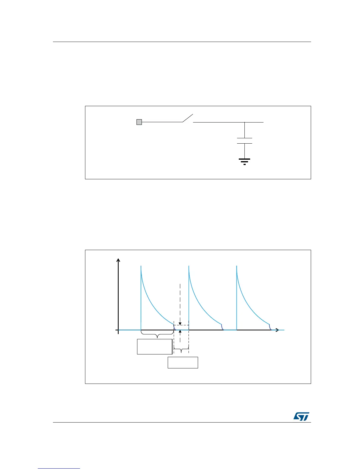
Figure 33 shows a simplified schematic of the input stage (sample and hold circuit).
Figure 33. ADC simplified schematic of input
stage - sample and hold circuit
The spikes (noise) present on ADC input pin during conversions are related to the sampling
switch (S
1
). If the switch is closed, some charge (coming from the sample and hold
capacitor C
sh
or caused by another effect) is transferred to the input pin. Then this charge
starts discharging through the source impedance (R
in
). The discharge process ends at the
end of the sampling time (t
S
) when the switch S
1
is opened. The remaining undischarged
voltage remains on the capacitor C
sh
and ADC measures this voltage. If the sampling time
(t
S
) is too short, the remaining voltage does not drop under 0.5 LSB and ADC measurement
shows an additional error. Figure 34 illustrates this process.
Figure 34. ADC input pin noise spikes from internal charge during sampling process
Note that a non-zero external capacitance C
ext
(parasitic pin capacitance) also exists, so
during conversion time the pin capacitance is discharged through source impedance R
in
.

 Loading...


