ADC errors AN2834
12/49 DocID15067 Rev 3
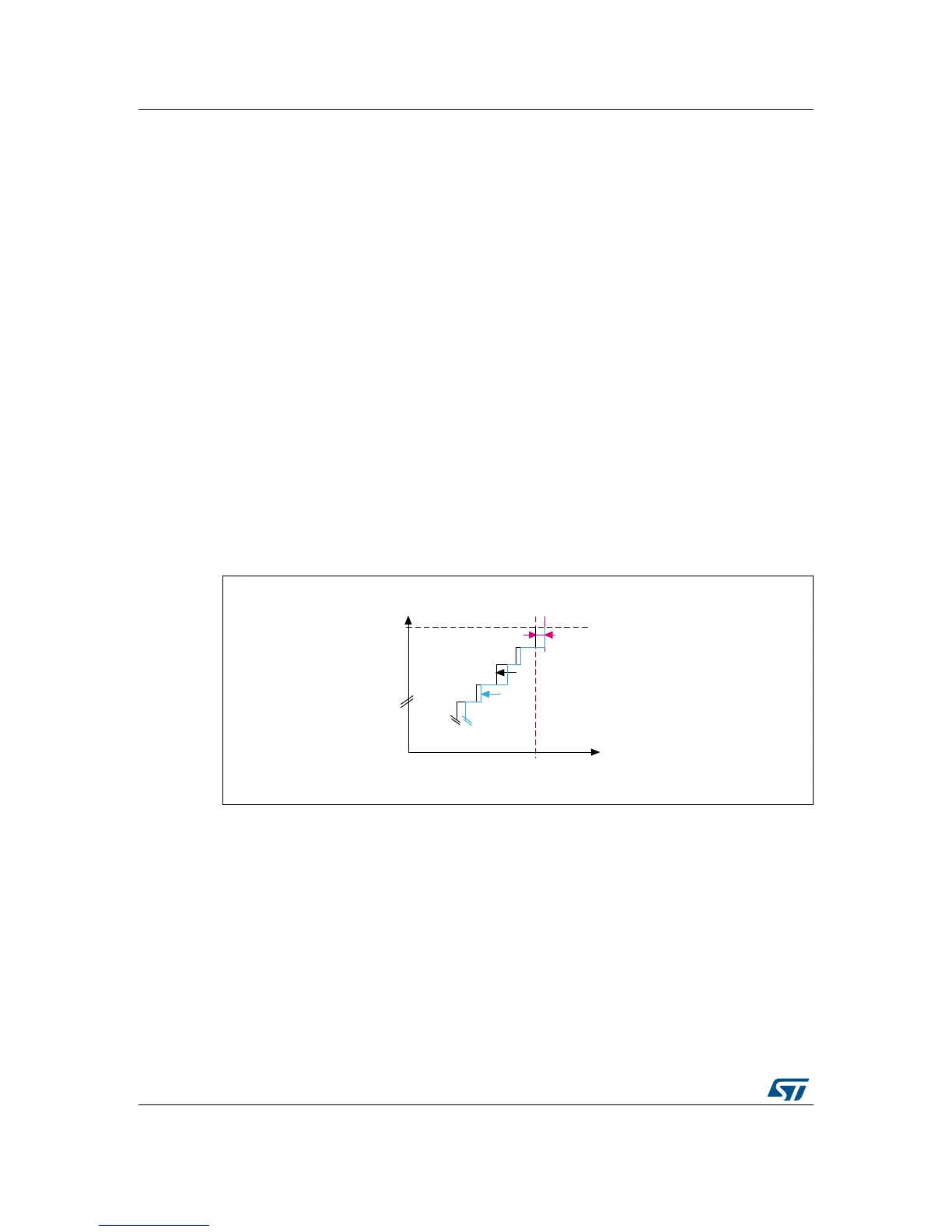
2.1.2 Gain error
The gain error is the deviation between the last actual transition and the last ideal transition.
It is denoted by E
G
.
The last actual transition is the transition from
0xFFE to 0xFFF. Ideally, there should be a
transition from 0xFFE to 0xFFF when the analog input is equal to V
REF+
– 0.5 LSB. So for
V
REF+
= 3.3 V, the last ideal transition should occur at 3.299597 V.
If the ADC provides the 0xFFF reading for V
AIN
< V
REF+
– 0.5 LSB, then a negative gain
error is obtained.
Example
The gain error is obtained by the formula below:
E
G
= Last actual transition – ideal transition
If V
REF+
= 3.3 V and V
AIN
= 3.298435 V generate a transition from 0xFFE to 0xFFF then:
E
G
= 3.298435 V – 3.299597 V
E
G
= –1162 µV
E
G
= (–1162 µV / 805.6 V) LSB = –1.44 LSB
If a full scale reading (0xFFF) is not obtained for V
AIN
equal to V
REF+
, the gain error is
positive. This means that a voltage greater than V
REF+
will cause the last transition. Figure 9
shows a positive gain error while Figure 10 shows a a negative gain error.
Figure 9. Positive gain error representation
1. The gain error, E
G
, is shown in magenta.
 Loading...


