How to get the best ADC accuracy AN2834
46/49 DocID15067 Rev 3
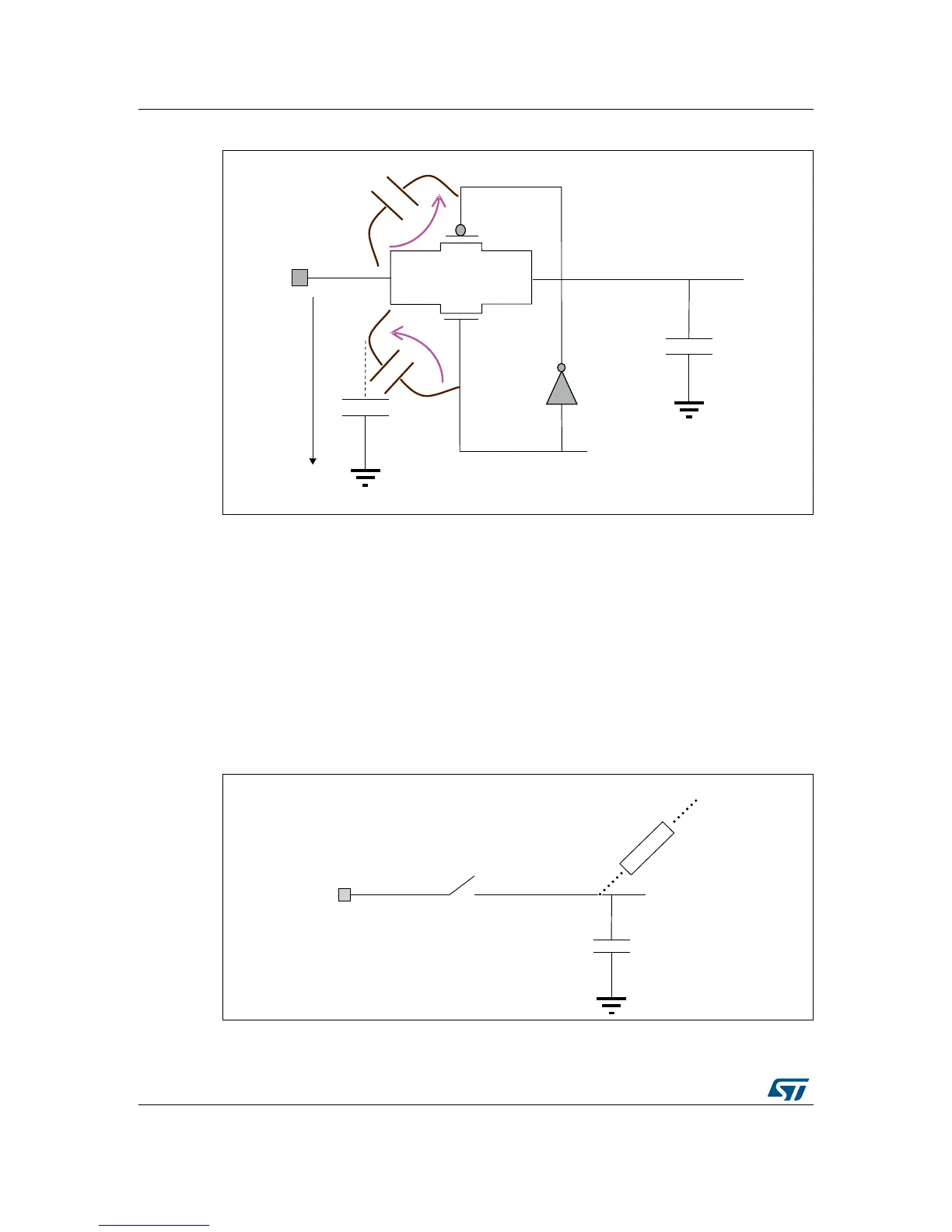
Figure 38. Parasitic capacitances of sampling switch
This charging and discharging currents (PMOS and NMOS asymmetric capacitances) can
cause charge transfer to sampling capacitor C
sh
.
Internal charging of sampling capacitor
It is possible that after the conversion process (successive approximation process in SAR
type of ADC) the sample and hold capacitor C
sh
is charged to some voltage. The reason
can be:
• some leakage current to C
sh
(parasitic current inside ADC structure, see Figure 39)
• residual charge transfer from the switches when ADC structure is switched back to
default state before next conversion
• other reasons (related to internal ADC parasitic structures)
Figure 39. Parasitic current example inside ADC structure

 Loading...