DocID15067 Rev 3 31/49
AN2834 How to get the best ADC accuracy
48
3.2.8 Temperature-effect compensation
One method is be to fully characterize the offset and gain drift and provide a lookup table in
memory to correct measurement according to temperature change. This calibration involves
additional cost and takes time.
The second method consists in recalibrating the ADC when the temperature change
re
aches given values, by using the internal temperature sensor and the ADC watchdog.
3.2.9 Minimizing injection current
Check the application to verify whether any digital or analog input voltage can be less than
V
SS
or V
SSA
. If it is the case, a negative injection current will flow from the pins. The effect
on the accuracy will be greater if a digital input is close to the analog input being converted.
Negative current injection on any of the standard (non-robust) analog input pins should be
av
oided as this would significantly reduce the accuracy of the conversion being performed
on another analog input.
It is recommended to connect a Schottky diode between V
SSA
and the I/O pin that can give
birth to the negative injection current.
The ADC accuracy will not be affected by posi
tive injection currents within the limits
specified for I
INJ(PIN)
and ΣI
INJ(PIN)
(refer to the appropriate STM32 datasheet, I/O port
characteristics section).
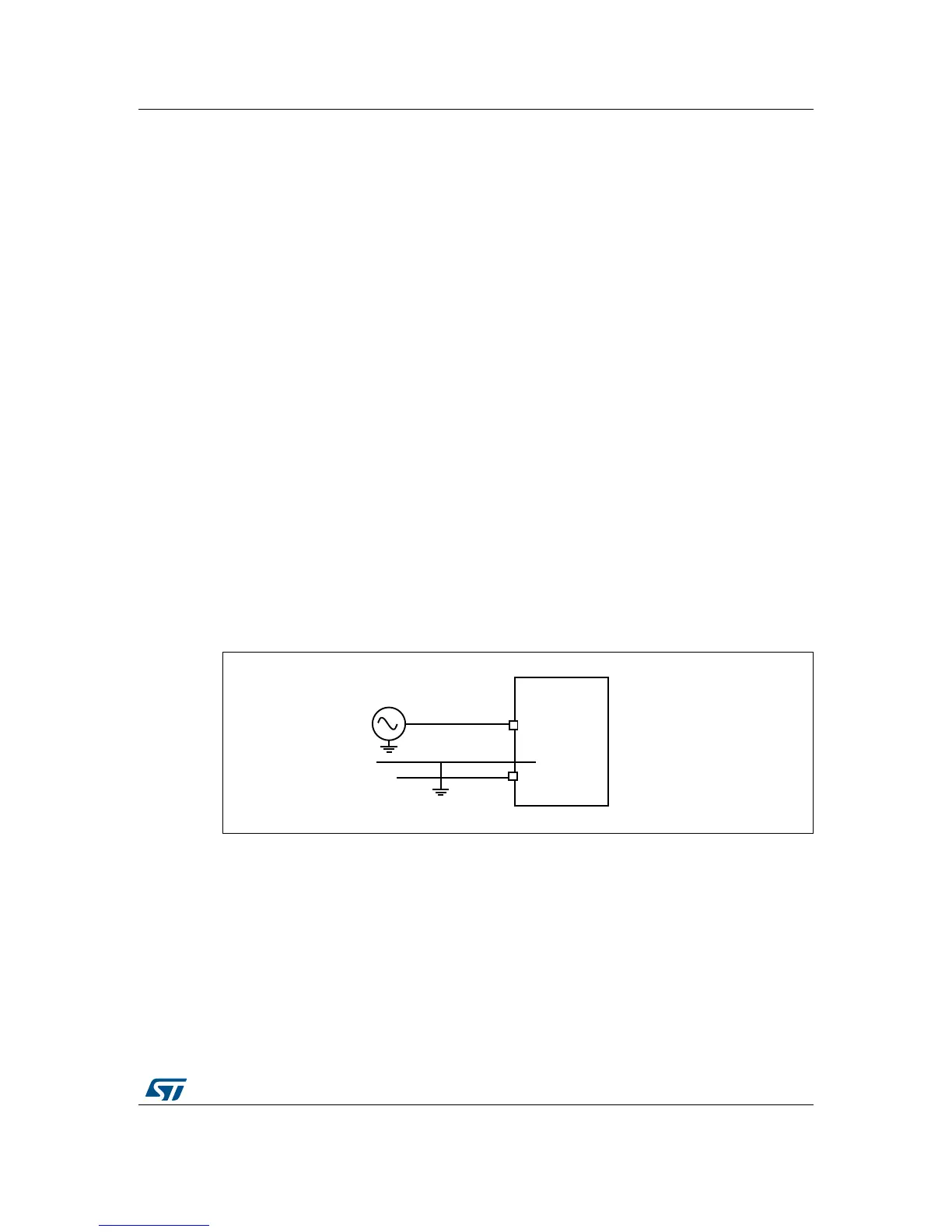
3.2.10 Minimizing I/O pin crosstalk
The noise produced by crosstalk can be reduced by shielding the analog signal by placing
ground tracks across it. Figure 27 shows the recommended grounding between signals.
Figure 27. Crosstalk between I/O pins

 Loading...


