DocID15067 Rev 3 19/49
AN2834 ADC errors
48
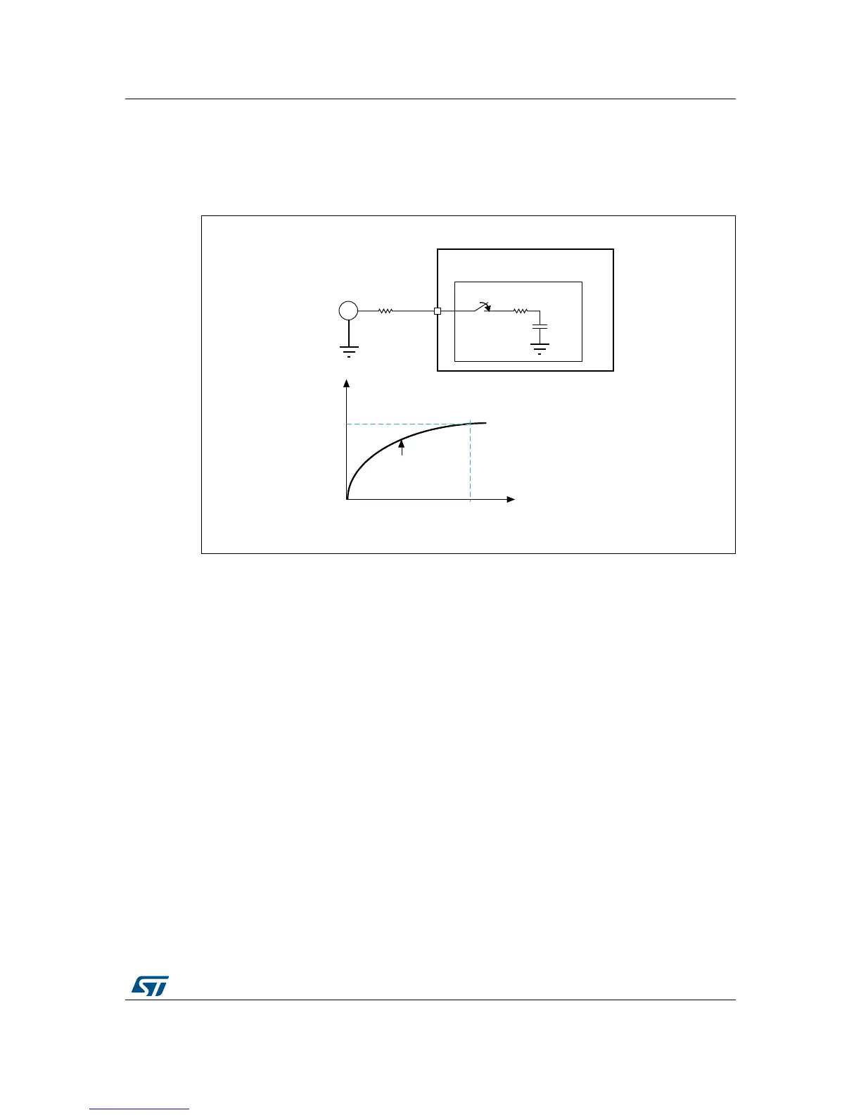
The effective charging of C
ADC
is governed by R
ADC
+ R
AIN
, so the charging time constant
becomes t
c
= (R
ADC
+R
AIN
) × C
ADC
. If the sampling time is less than the time required to fully
charge the C
ADC
through R
ADC
+ R
AIN
(t
s
< t
c
), the digital value converted by the ADC is
less than the actual value.
Figure 15. Analog signal source resistance effect
1. t
c
is the time taken by the C
ADC
capacitor to fully charge: V
c
= V
AIN
(with max.1/2 LSB error)
V
c
: capacitor (C
ADC
) voltage
t
c
= (R
ADC
+ R
AIN
) × C
ADC
2.2.7 Effect of source capacitance and parasitic capacitance of the PCB
When converting analog signals, it is necessary to account for the capacitance at the source
and the parasitic capacitance seen on the analog input pin (refer to Figure 16). The source
resistance and capacitance form an RC network. In addition, the ADC conversion results
may no
t be accurate unless the external capacitor (C
AIN
+ C
p
) is fully charged to the level of
the input voltage. The greater value of (C
AIN
+ C
p
), the more limited the source frequency.
The external capacitance at the source and the parasitic capacitance are denoted by C
AIN
and C
p
, respectively.

 Loading...


