How to get the best ADC accuracy AN2834
34/49 DocID15067 Rev 3
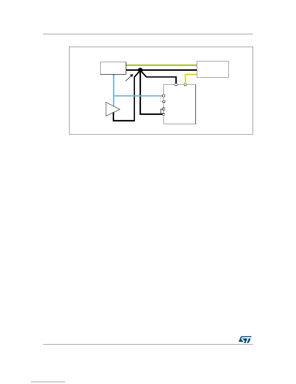
Figure 30. Separating the analog and digital supplies
It is also recommended to connect the analog and digital grounds in a star network. This
means that you must connect the analog and digital grounds at only one point. This
prevents the introduction of noise in the analog power supply circuit due to digital signal
switching. This also prevents current surges from affecting the analog circuit.
Using separate PCB layers for the supply and ground
• Two-layer PCBs
For two-layer PCBs, it is recommended to provide a maximum ground plane area. The
power supply (V
DD
, V
DDA
) should run through thick tracks. The two layers can have
their ground shorted together via multiple connections in the overlap region if the two
layers feature the same ground signals. The unused PCB area can be used as the
ground plane.
The other convention is to connect the unused PCB area on one layer to the positive
supply (V
DD
) and the unused area on the other layer, to ground. The advantage is a
reduced inductance for power and ground signals. The maximum ground area provided
for ground on the PCB results in a good shielding effect and reduces the
electromagnetic induction susceptibility of the circuit.
• Multilayer PCBs
Wherever possible, try to use multilayer PCBs and use separate layers on the PCB for
power and ground. The V
DD
and V
SS
pins of the various devices can be directly
connected to the power planes, thus reducing the length of track needed to connect the
supply and ground. Long tracks have a high inductive effect. The analog ground can be
connected at one point to this ground plane. If so, it should be close to the power
supply.
A full ground plane provides good shielding and reduces the electromagnetic induction
susceptibility of the circuit.
• Single-layer PCBs
Single-layer PCBs are used to save cost. They can be used only in simple applications
when the number of connections is very limited. It is recommended to fill the unused
area with ground. Jumpers can be used to connect different parts of the PCB.

 Loading...


