ADC errors AN2834
18/49 DocID15067 Rev 3
2.2.3 External reference voltage parameters
In case of usage external source for reference voltage (on V
REF+
pin) there are important
parameters of this external reference source. Three reference voltage specifications must
be considered: temperature drift, voltage noise, long term stability.
2.2.4 Analog input signal noise
Small but high-frequency signal variation can result in big conversion errors during sampling
time. This noise is generated by electrical devices, such as motors, engine ignition, power
lines. It affects the source signal (such as sensors) by adding an unwanted signal. As a
consequence, the ADC conversion results are not accurate.
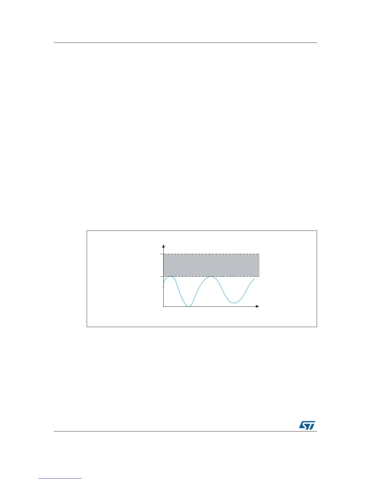
2.2.5 ADC dynamic range bad match for maximum input signal amplitude
To obtain the maximum ADC conversion precision, it is very important that the ADC dynamic
range matches the maximum amplitude of the signal to be converted. Let us assume that
the signal to be converted varies between 0 V and 2.5 V and that V
REF+
is equal to 3.3 V.
The maximum signal value converted by the ADC is 3102 (2.5 V) as shown in Figure 14. In
this case, there are 993 unused transitions (4095 – 3102 = 993). This implies a loss in the
converted signal
accuracy.
See Section 3.2.5: Matching the ADC dynamic r
ange to the maximum signal amplitude on
page 26 for details on how to make the ADC dynamic range match the maximum input
signal amplitude.
Figure 14. Input signal amplitude vs. ADC dynamic range
2.2.6 Effect of the analog signal source resistance
The impedance of the analog signal source, or series resistance (R
AIN
), between the source
and pin, causes a voltage drop across it because of the current flowing into the pin. The
charging of the internal sampling capacitor (C
ADC
) is controlled by switches with a
resistance R
ADC
.
With the addition of source resistance (with R
ADC
), the time required to fully charge the hold
capacitor increases. Figure 15 shows the analog signal source resistance effect.

 Loading...


