FN990
Family Hardware Design Guide
1VV0301752 Rev. 3 Page 16 of 92 2022-10-07
Not Sub
ect to NDA
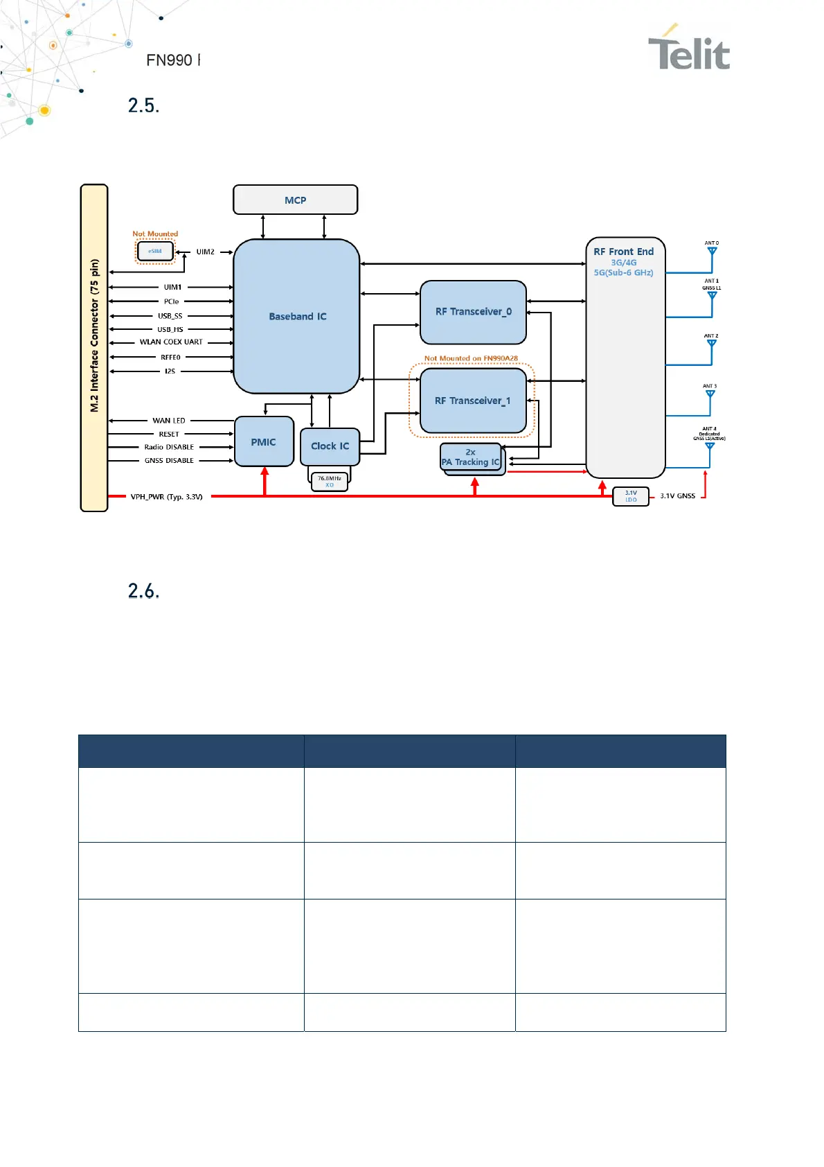
Block Diagram
The figure below shows an overview of the internal architecture of the FN990 Family
module.
Figure 1: FN990 Family Block Diagram
RF Performance
The RF performance in 5G, LTE and WCDMA modes conforms to the 3GPP specifications.
2.6.1. Conducted Transmit Output Power
TX power follows the measurement conditions and specifications defined in 3GPP.
Band Power class RF Power (dBm)
5G NR Sub-6
n1, n2, n3, n5, n7, n8, n20, n25, n28,
n30, n38, n40, n41, n48, n66, n71, n77,
n78, n79
3 (0.2W) 23 (+2dB / -2dB)
5G NR Sub-6
n41, n77, n78, n79
Supports Power Class 2
2 (0.4W) 26 (+2dB / -2dB)
LTE All Bands
B1, B2, B3, B4, B5, B7, B8, B12, B13,
B14, B17, B18, B19, B20, B25, B26,
B28, B30, B34, B38, B39, B40, B41,
B42, B43, B48, B66, B71
3 (0.2W) 23 (+2dB / -2dB)
LTE B41
Supports Power Class 2
2 (0.4W) 26 (+2dB / -2dB)
 Loading...