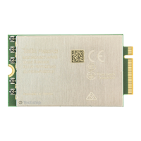
FN990
Family Hardware Design Guide
1VV0301752 Rev. 3 Page 91 of 92 2022-10-07
Not Sub
ect to NDA
14. DOCUMENT HISTORY
Revision Date Changes
3 2022-10-07 Section 2.2.1 Updated Frequency Bands
Section 2.6 Updated RF Performance
Section 2.4 PCIe Gen 4 -> PCIe Gen 3
Section 3.1 Updated 3.1 Pin-out
Section 3.3 Updated 3.3 Pin Layout
Section 4.2 Updated Power consumption
Section 6.3.1.2.1 Added PCIe Layout Guidelines
Section 6.3.1.3.1 Added USB Layout Guidelines
Section 6.4 Updated General Purpose I/O
Section 7.1.1 Updated Antenna Configuration
Section 7.2 Updated Antenna Connector
Section 8.4 Solder Resist Opening Area and Keepout Area added
Section 11. Updated CONFORMITY ASSESTMENT ISSUES
Section 13. Updated Glossary
2 2022-06-09 Section 6.2 Updated Power ON/OFF/RESET
Section 2.4, 6.3.2, 6.3.3 Updated eSIM description
Section 4.2 Updated Power consumption
Section 2.6.2 Conducted Receiver Sensitivity
1 2022-04-22 Section 2.4 Updated Processor Clock
Section 3.1 Updated Pin-out
Section 3.3 Updated Pin Layout
Section 4.1 Updated Power Supply Requirements
Section 4.2 Updated LPM Power Consumption
Section 6.1 Updated I/O Operating Range
Section 6.2 Updated Power ON/OFF/RESET
Section 6.3 Added and updated information about interfaces
0 2021-12-16 First Draft
From Mod.0818 rev.2

 Loading...