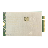
FN990
Family Hardware Design Guide
1VV0301752 Rev. 3 Page 3 of 92 2022-10-07
Not Sub
ect to NDA
CONTENTS
APPLICABILITY TABLE 2
CONTENTS 3
1.
INTRODUCTION 8
Scope 8
Audience 8
Contact Information, Support 8
Symbol Conventions 9
Related Documents 9
2.
GENERAL PRODUCT DESCRIPTION 10
Overview 10
Frequency Bands and CA / EN-DC Combinations 10
2.2.1.
Frequency Bands 10
2.2.2.
CA / MIMO / EN-DC 13
Target Market 13
Main Features 14
2.4.1.
Configurations Pins 15
Block Diagram 16
RF Performance 16
2.6.1.
Conducted Transmit Output Power 16
2.6.2.
Conducted Receiver Sensitivity 17
Mechanical Specifications 20
2.7.1.
Dimensions 20
2.7.2.
Weight 20
Environmental Requirements 20
2.8.1.
Temperature Range 20
2.8.2.
RoHS Compliance 21
3.
PINS ALLOCATION 22
Pin-out 22
FN990 Family Signals That Must be Connected 25
Pin Layout 26
 Loading...