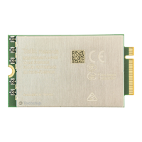
FN990
Family Hardware Design Guide
1VV0301752 Rev. 3 Page 4 of 92 2022-10-07
Not Sub
ect to NDA
4.
POWER SUPPLY 27
Power Supply Requirements 27
Power Consumption 27
General Design Rule 28
4.3.1.
Electrical Design Guidelines 29
4.3.1.1.
+5V Source Power Supply Design Guidelines 29
4.3.2.
Thermal Design Guidelines 29
4.3.3.
Power Supply PCB Layout Guidelines 30
RTC 31
Reference Voltage 31
Internal LDO for GNSS Bias 31
5.
ELECTRICAL SPECIFICATIONS 32
Absolute Maximum Ratings – Not Optional 32
Recommended Operating Conditions 32
6.
DIGITAL SECTION 33
Logic Levels 33
6.1.1.
1.8V Pins – Absolute Maximum Ratings 33
6.1.2.
1.8V Standard GPIOs 33
6.1.3.
1.8V UIM1/UIM2 Pins 33
6.1.4.
2.95V Pins – Absolute Maximum Ratings 34
6.1.5.
2.95V SIM Card Pins 34
6.1.6.
VPH_PWR Level I/O Pins 34
Power ON/OFF/RESET 34
6.2.1.
Power On 35
6.2.1.1.
Initialization and Activation State 35
6.2.2.
Power Off 38
6.2.2.1.
Graceful Shutdown 39
6.2.2.2.
Fast Shutdown 40
6.2.3.
Reset 42
6.2.3.1.
Unconditional Hardware Reset 42
Communication Ports 44
6.3.1.
Host Interface 44

 Loading...