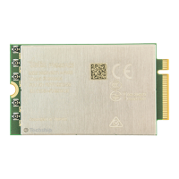
FN990
Family Hardware Design Guide
1VV0301752 Rev. 3 Page 30 of 92 2022-10-07
Not Sub
ect to NDA
Note: There is the large solder resist opening area on the bottom side
of the module. Adding a TIM on that area with a heatsink is highly
recommended to ensure proper heat dissipation.
The modem temperature vale can be read via AT command.
Note: For optimal RF performance, thermal dissipation and
mecahnical stability, the FN990 must be connected to the ground and
metal chassis of the host board.
The module shield and host device or metal chassis of the host device
should be connected by means of conductive material.
4.3.3. Power Supply PCB Layout Guidelines
As described in the electrical design guidelines, a low ESR capacitor should be connected
to the power supply output to reduce current peaks. A protection diode on the modem
power supply input should be connecte to protect the FN990 from spikes and polarity
inversion.
Placement of these components is crucial for correct operation: a misplaced component
can badly affect power supply performance:
The bypass low ESR capacitor must be placed close to the FN990 power input pins
or - if the power supply is of a switching type - it can be placed close to the inductor
to reduce ripple, as long as the PCB trace from the capacitor to FN990 is wide
enough to avoid significant voltage drop even during the 4A current peaks.
The protection diode must be placed close to the modem connector.
The PCB traces from the input connector to the power regulator IC must be wide
enough to ensure that no voltage drops occur during the 4A current peaks.
The PCB traces connecting the FN990 and bypass capacitor must be wide enough
to avoid voltage drops even when 4A current absorbtion peaks occur. These traces
should be kept as short as possible.
The PCB traces connecting the switching output to the inductor and the switching
diode must be kept as short as possible by placing the inductor and the diode as
closed as possible to the power switching IC (only for the switching power
supplies). This is done to reduce the radiated field (noise) at the switching
frequency (usually 100-500 kHz).

 Loading...