FN990
Family Hardware Design Guide
1VV0301752 Rev. 3 Page 28 of 92 2022-10-07
Not Sub
ect to NDA
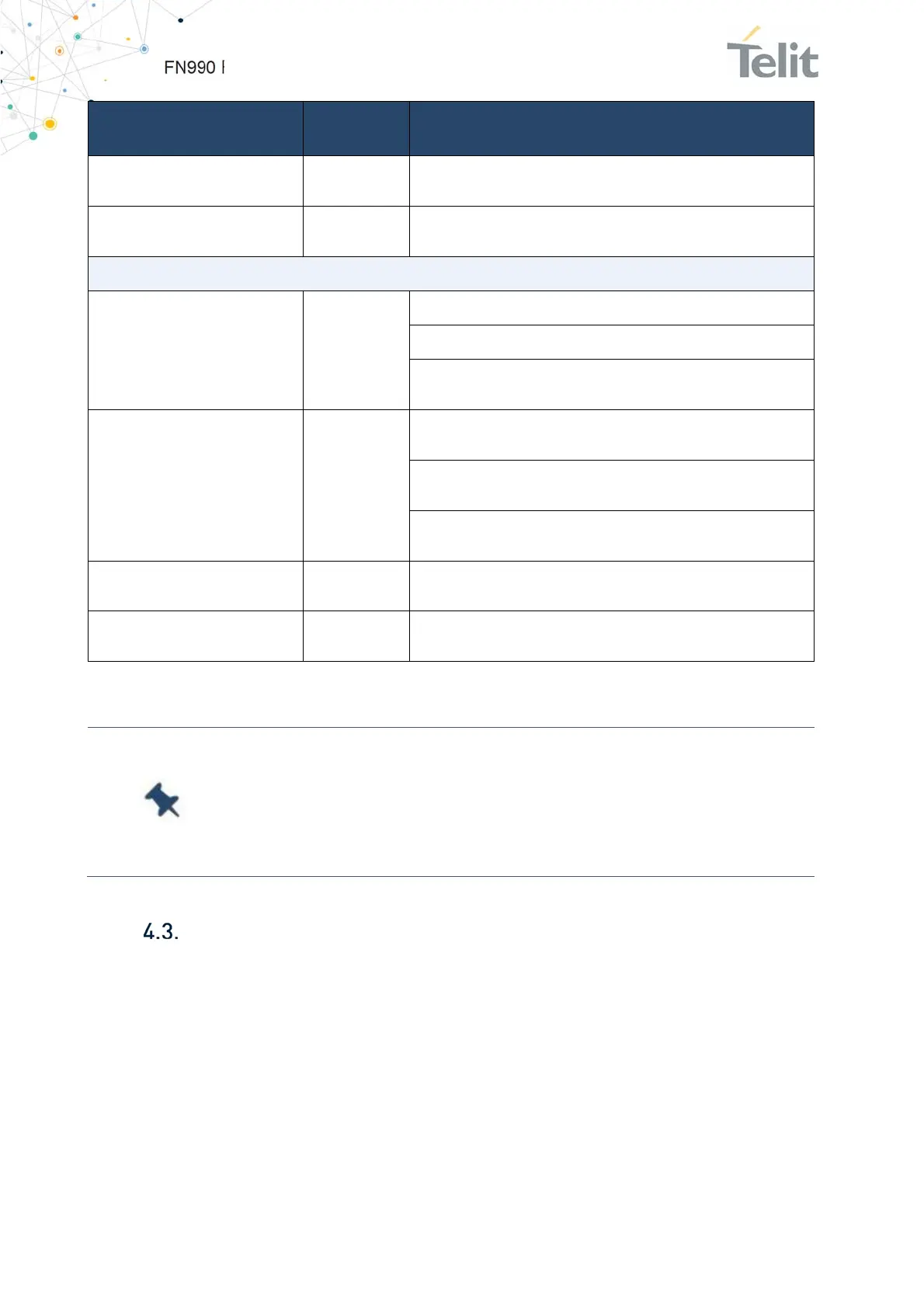
Mode
Average
[Typ.]
Mode Description
7DLCA (4x4,2x2MIMO) with
1UL(SISO)
1450mA
CA_1A-3C-7C-20A-38A, Full RB, 256QAM DL/ 256QAM
UL(1500Mbps DL / 103Mbps UL)
5DLCA (4x4MIMO) with
1UL(SISO)
1150mA
CA_1A-3C-7C, Full RB, 256QAM DL/ 256QAM UL(2Gbps DL /
103Mbps UL)
Operative Mode (NR-FR1)
NSA mode
1CC+1FR1
900 mA
EN-DC_1A(1DL/UL SISO)-n78A(1DL/1UL SISO)
LTE : BW 20MHz, 1 RB, QPSK DL / QPSK UL, 23dBm
FR1 : BW 100MHz, Inner RB 137(Number)@64(Position), QPSK
DL / QPSK UL, 23 dBm
NSA mode
6CC+1FR1
2000mA
EN-DC_1A(DL2x2/1UL SISO)-3C(DL4x4)-
7C(DL4x4)_28A(DL2x2) -n78(1DL 4x4MIMO/1UL SISO/60M)
LTE : BW 20MHz, Full RB, 256QAM DL / 256QAM UL(2Gbps DL
/ 103Mbps UL)
FR1 : BW100MHz, Full RB, 256QAM DL / 256QAM UL(1.6Gbps
DL/118Mbps)
SA mode 1FR1 380mA
FR1(n78A) : BW100MHz, Full RB, 256QAM DL / 256QAM
UL(1.89Gbps DL/1.25Mbps)
SA mode 2FR1 730mA
FR1(CA_n78A_n78A) : BW200MHz, Full RB, 256QAM DL /
256QAM UL(3.8Gbps DL/1.25Mbps)
Table 16: FN990 Family Current Consumption
Note: Worst/best case current consumption values depend on
mobile network configuration – not under module control.
* Loop-back mode in call equipment
* 3.3 voltage / room temperature
General Design Rule
The principal guidelines for the Power Supply Design include three different design steps:
Electrical design
Thermal design
PCB layout
 Loading...